
Author: Farid M, https://embeddeddesign.org/
In this article, I will talk about a six pulse three phase AC-DC converter design I implemented on a Xilinix FPGA, Zynq-7000: https://amzn.to/2CZakDI. The converter uses semiconductor controller rectifiers, SCRs, to generate +24VDC output voltage. Before I start talking about how the digital control algorithm is implemented in VHDL, I would like first to talk a bit about SCRs and how they work.
An SCR is a device made of four layers of alternating N-type and P-type semiconductor material. As seen in the diagram below, an SCR has three terminals: Gate, Anode and cathode and current flows through it only in the positive direction: from Anode to Cathode. An SCR can be turned on in two ways: either by applying an increasing voltage between the anode and cathode till it gets beyond the breakdown voltage or by sending a positive pulse at the gate, which is the case in this project.
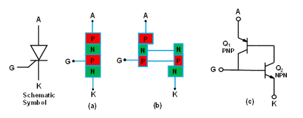
Figure1. Semiconductor Controlled Rectifier: https://amzn.to/2SIxSly
Theoretically, the DC output voltage of a three phase full-wave SCR bridge rectifier is a function of what it is called: SCR firing time delay, which is a phase delay between the moment an AC phase signal changes polarity from positive to negative or negative to positive, and the rising edge of the positive gate pulse.
In my design each AC phase signal goes through an analogue Zero Crossing Detection circuit, ZCD. As soon as the AC signal change polarity in either direction, an active high pulse is generated. Since I am having a system powered up from a three phase power source, this means I will have six zero crossing detection pluses generated at different times: 2 pulses per one phase cycle. The rising edge of each of these pulses will be used trigger a timer counter for the phase delay. Once this timer expires, depending on the phase angle required, a pulse is sent to the gate of its dedicated thyristor.
The schematics below shows the circuit implementation of this three phase full wave controlled rectifier. By looking at Figure2 and figure3, which shows power source that is the three phase signals, I will explain the firing sequence for each rectifier thyristor: T1,T2,T3,T4, T5, and T6. I would like to mention here that the purple, green and red waveforms represent Phase A, Phase B, and Phase C respectively.

Figure2. Fullwave SCR AC-DC converter schematics
 Figure3. Three phase AC Signals: 120º phase with each other
Each of the six SCRs are turned on when these two conditions occur:
- When a phase power signal changes polarity from positive to negative or from negative to positive. In other words, when a zero crossing detect signal becomes active high.
- When firing time delay is expired: 60º +α(the firing phase delay). In this demo project, I selected a phase delay α=0º.
The offset 60º is used here when we do not have access to the Neutral line, meaning the load is connected as shown in Figure2. But if we have access to the Neutral line and the negative terminal of the load, for example a battery, is connected to neutral line while positive terminal is connected to positive output port, then the offset is equal to 30º, and in this case the firing angle delay will be 30º +α.
The SCRs firing pulses sequence, assuming no access to the neutral line: Pulses are sent after α+60º from the time a zero crossing detect signal becomes active high. For a 50 Hz AC power signal, this means that for a phase delay angle α=0º, the time delay is equal to 60*20/360=3.33ms. Below is the firing sequence of all the thyristors gate pulses:
- T1 is triggered by Pulse1 after 3.33ms (60º+α) from the instance V_an (Phase A) changes polarity from positive to negative.
- T2 is triggered by Pulse2 after 3.33ms (60º+α) from the instance V_cn (Phase C) changes polarity from positive to negative.
- T3 is triggered by Pulse3 after 3.33ms (60º+α) from the instance V_bn (Phase B) changes polarity from negative to positive.
- T4 is triggered by Pulse4 after 3.33ms (60º+α) from the instance V_an (Phase A) changes polarity from positive to negative.
- T5 is triggered by Pulse5 after 3.33ms (60º+α) from the instance V_Cn (Phase C) changes polarity from negative to positive.
- T6 is triggered by Pulse6 after 3.33ms (60º+α) from the instance V_bn (Phase B) changes polarity from positive to negative.
Another important requirement to mention here is the pulse width. It is very important to have the pulse ON for an adequate amount of time so that the SCR is energized properly. Regardless of having access to neutral or not,the maximum pulse duration is 120º. Thus in our example, the pulse duration formula is always: 180º-(60º+α), and this means that for α=0º, the pulse duration will be 120º or 6.67ms. Please, note that this pulse duration will get shorter more and more as the delay angle α increases. For example, for an α=90º, the pulse duration will be: 30º or 1.67ms. However, with neutral line as the load reference, the falling edge of the firing pulse will always occurs at 150º from the zero crossing, while, in our example( no access to neutral line) this pulse falling edge will always occur at 180º from the zero crossing event.
The diagram below shows the the six firing pulses for: T1 (probe0), T2(probe1), T3(probe2), T4(probe3), T5(probe4), and T6(probe5). Notice the duration of the pulse when it is high: since my system runs from a three phase 50 Hz source, 120 degrees corresponds to 6.67ms, which is roughly the case on my scope if I had increased my time resolution. Also notice in Figure5 that the phase delay between all pulses is 60º.
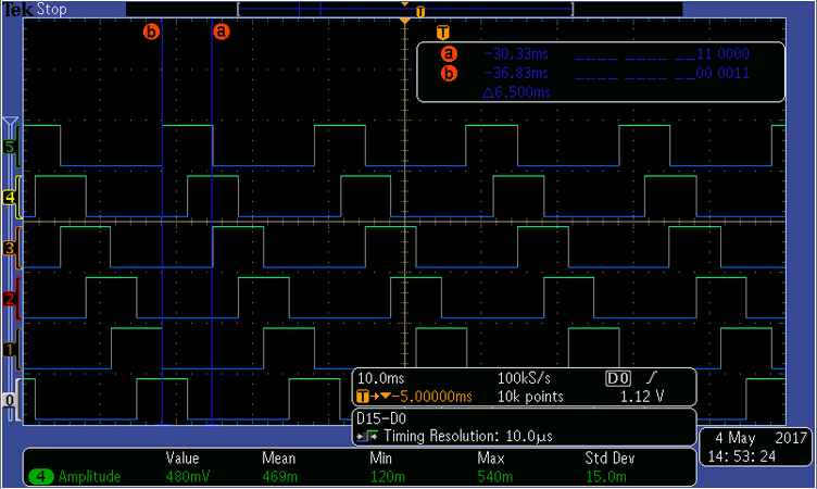 Figure4: Six SCR Firing Pulses for a phase angle α=0 degrees
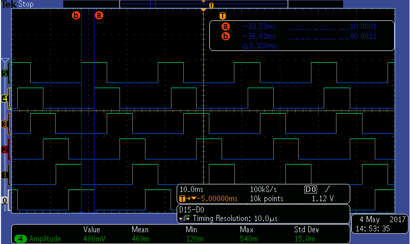 Figure5: Angle phase delay for α=0 degrees
In the next few paragraphs, I will be explaining how the code is implemented in VHDL. The project is implemented on a Xilinix Zedboard: https://amzn.to/2CZakDI, and it uses AXI protocol to transfer data from the processor system, PS, to the peripheral logic, PL, via UART. In this project, the user makes a selection of the phase delay desired: α=0º, α=30º, α=45º, α=60º, α=75º, α=90º, and the generated DC output is displayed onto an LCD. Below are the main processes of the SCRs control algorithm.
VHDL Implementation
Phase Selection: This process gives the user the option to select the desired phase angle delay. Note here that the system frequency used is 100MHz, and a full power cycle is completed every 20 ms: when counter=2000000. Note here that “phaseSelect” register is updated from the PS via AXI protocol.
PhaseSELECTION: process(clock,reset)
begin
if(reset='1') then
  FiringPulse_RisingEdge<=0;
  FiringPulse_FallingEdge<=0;
 elsif(rising_edge(clock)) then
   if(phaseSelect="000001") then     --zero degrees delay
     FiringPulse_RisingEdge<=333333; --0+60 degrees: pulse duration=120degrees(6.67ms)
     FiringPulse_FallingEdge<=1000000; --120 degrees +60 degrees
   elsif(phaseSelect="000010")then     --15 degrees degrees delay:pulse duration=105degrees(5.83ms)
     FiringPulse_RisingEdge<=416667;
     FiringPulse_FallingEdge<=1000000;
   elsif(phaseSelect="000100")then     --30 degrees degrees delay:pulse duration=90degrees(5ms)
      FiringPulse_RisingEdge<=500000;
      FiringPulse_FallingEdge<=1000000;
   elsif(phaseSelect="001000")then      --45 degrees degrees delay: pulse duration=75degrees(4.16ms)
       FiringPulse_RisingEdge<=583333;
       FiringPulse_FallingEdge<=1000000;
   elsif(phaseSelect="010000")then     --60 degrees degrees delay: pulse duration=60degrees(3.33ms)
       FiringPulse_RisingEdge<=666667;
       FiringPulse_FallingEdge<=1000000;
   elsif(phaseSelect="010000")then      --75 degrees degrees delay: pulse duration=45degrees(2.5ms)
       FiringPulse_RisingEdge<=750000;
       FiringPulse_FallingEdge<=1000000;
    elsif(phaseSelect="100000")then       --90 degrees degrees delay: pulse duration=30degrees(1.67ms)
        FiringPulse_RisingEdge<=833333;
        FiringPulse_FallingEdge<=1000000;
     else
        FiringPulse_RisingEdge<=333333;    --zero degrees delay
        FiringPulse_FallingEdge<=1000000;
     end if;

end if;
end process PhaseSELECTION
Timer counters Process: This process is used to implement a timer for phase delay whenever a zero crossing detection signal becomes active high.
TimerCounters:process (clock,reset)
begin
if(reset='1') then
   PhaseCounter1<=0;
   PhaseCounter2<=0;
   PhaseCounter3<=0;
   PhaseCounter4<=0;
   PhaseCounter5<=0;
   PhaseCounter6<=0;
   SynchFlag<="000000";
elsif(rising_edge(clock)) then
 PhaseCounter1<=PhaseCounter1+1;
  if(SW1_CrossUp_Pulse='1')then
     PhaseCounter1<=0;        --Reset counter1
     SynchFlag(0)<='1';
end if;
PhaseCounter2<=PhaseCounter2+1;
 if(SW3_CrossDwn_Pulse='1')then
    PhaseCounter2<=0;        --Reset counter2
    SynchFlag(1)<='1';
 end if;
PhaseCounter3<=PhaseCounter3+1;
if(SW2_CrossUp_Pulse='1')then
   PhaseCounter3<=0;       --Reset counter3
   SynchFlag(2)<='1';
end if;
PhaseCounter4<=PhaseCounter4+1;
if(SW1_CrossDwn_Pulse='1')then
   PhaseCounter4<=0;       --Reset counter4
   SynchFlag(3)<='1';
end if;
PhaseCounter5<=PhaseCounter5+1;
if(SW3_CrossUp_Pulse='1')then
   PhaseCounter5<=0;       --Reset counter5
   SynchFlag(4)<='1';
end if;
PhaseCounter6<=PhaseCounter6+1;
if(SW2_CrossDwn_Pulse='1')then
  PhaseCounter6<=0;         --Reset counter6
  SynchFlag(5)<='1';
end if;

end if;
end process counters;
SCR Control Process: This process controls the firing sequence of each SCR.
SCRs_Control:process (clock,reset)
begin
if(reset='1') then
  Thyristors_Sig'0');
elsif(rising_edge(clock)) then
   --Thyristor T1 Control --PhaseA_CrossUp='1'
   if(PhaseCounter1=FiringPulse_RisingEdge) then
     Thyristors_Sig(0)<='1';
   elsif(PhaseCounter1=FiringPulse_FallingEdge)then
     Thyristors_Sig(0)<='0';
   end if;
   ---Thyristor T2 Control --Phase3_CrossDwn='1'
   if(PhaseCounter2=FiringPulse_RisingEdge) then
     Thyristors_Sig(1)<='1';
   elsif(PhaseCounter2=FiringPulse_FallingEdge)then
     Thyristors_Sig(1)<='0';
   end if;
   --Thyristor T3 Control --PhaseB_CrossUp='1'
   if(PhaseCounter3=FiringPulse_RisingEdge) then
     Thyristors_Sig(2)<='1';
   elsif(PhaseCounter3=FiringPulse_FallingEdge)then
     Thyristors_Sig(2)<='0';
   end if;
   --Thyristor T4 Control --PhaseA_CrossDwn='1'
   if(PhaseCounter4=FiringPulse_RisingEdge) then
     Thyristors_Sig(3)<='1';
   elsif(PhaseCounter4=FiringPulse_FallingEdge)then
     Thyristors_Sig(3)<='0';
   end if;
   --Thyristor T5 Control --PhaseC_CrossUp='1'
   if(PhaseCounter5=FiringPulse_RisingEdge) then
    Thyristors_Sig(4)<='1';
   elsif(PhaseCounter5=FiringPulse_FallingEdge)then
    Thyristors_Sig(4)<='0';
   end if;
   --Thyristor T6 Control --PhaseB_CrossDwn='1'
  if(PhaseCounter6=FiringPulse_RisingEdge) then
    Thyristors_Sig(5)<='1';
  elsif(PhaseCounter6=FiringPulse_FallingEdge)then
    Thyristors_Sig(5)<='0';
  end if;
 end if;
end process;
-------------------------------------------------------------------
VHDL Simulation for a Six Pulses Three Phase Controlled Rectifier
The VHDL processes below simulates a three phase AC power system running at 50 Hz. Also it simulates six thryistors firing at α=0º. Complete VHDL file can be downloaded from my Github repository at: here
The three phase sine waveform were generated using a look up table as shown below:
type SineConstants_Array is array(0 to 399) of integer range -1241 to 1241; --signed(12 downto 0); --400 constants 11 bits each
constant SineConstants : SineConstants_Array :=
(19,39,58,78,97,117,136,156,175,194,213,233,252,271,290,309,328,346,365,
384,402,420,439,457,475,493,511,528,546,563,581,598,615,632,649,665,681,
698,714,730,745,761,776,791,806,821,835,850,864,878,891,905,918,931,944,
956,969,981,993,1004,1015,1027,1037,1048,1058,1068,1078,1088,1097,1106,
1115,1123,1131,1139,1147,1154,1161,1168,1174,1180,1186,1192,1197,1202,1207,
1211,1215,1219,1223,1226,1229,1231,1234,1236,1237,1239,1240,1241,1241,1241,
1241,1241,1240,1239,1237,1236,1234,1231,1229,1226,1223,1219,1215,1211,1207,
1202,1197,1192,1186,1180,1174,1168,1161,1154,1147,1139,1131,1123,1115,1106,
1097,1088,1078,1068,1058,1048,1037,1027,1015,1004,993,981,969,956,944,931,
918,905,891,878,864,850,835,821,806,791,776,761,745,730,714,698,681,665,649,
632,615,598,581,563,546,528,511,493,475,457,439,420,402,384,365,346,328,309,
290,271,252,233,213,194,175,156,136,117,97,78,58,39,19,0,-19,-39,-58,-78,
-97,-117,-136,-156,-175,-194,-213,-233,-252,-271,-290,-309,-328,-346,-365,
-384,-402,-420,-439,-457,-475,-493,-511,-528,-546,-563,-581,-598,-615,-632,
-649,-665,-681,-698,-714,-730,-745,-761,-776,-791,-806,-821,-835,-850,-864,
-878,-891,-905,-918,-931,-944,-956,-969,-981,-993,-1004,-1015,-1027,-1037,
-1048,-1058,-1068,-1078,-1088,-1097,-1106,-1115,-1123,-1131,-1139,-1147,
-1154,-1161,-1168,-1174,-1180,-1186,-1192,-1197,-1202,-1207,-1211,-1215,
-1219,-1223,-1226,-1229,-1231,-1234,-1236,-1237,-1239,-1240,-1241,-1241,
-1241,-1241,-1241,-1240,-1239,-1237,-1236,-1234,-1231,-1229,-1226,-1223,
-1219,-1215,-1211,-1207,-1202,-1197,-1192,-1186,-1180,-1174,-1168,-1161,
-1154,-1147,-1139,-1131,-1123,-1115,-1106,-1097,-1088,-1078,-1068,-1058,
-1048,-1037,-1027,-1015,-1004,-993,-981,-969,-956,-944,-931,-918,-905,-891,
-878,-864,-850,-835,-821,-806,-791,-776,-761,-745,-730,-714,-698,-681,-665,
-649,-632,-615,-598,-581,-563,-546,-528,-511,-493,-475,-457,-439,-420,-402,
-384,-365,-346,-328,-309,-290,-271,-252,-233,-213,-194,-175,-156,-136,-117,
-97,-78,-58,-39,-19,0);
Sine waves generation: This process generates three sine wave forms 120 degrees out of phase from each other running at 50 Hz. Signal Sine1_out, Sine2_out,and Sine3_out simulates Phase A, Phase B, and Phase C respectively. I selected the counter to reset at 5000 as I am running the FPGA at 100MHz.
--------------------------------------------------------------------------
--Sine waves generation:
--------------------------------------------------------------------------
SineWaves:process (clock,reset)
variable counter : integer range 0 to 5000;
begin
if(reset='1') then
Sine1_out<=0;
Sine2_out<=0;
Sine3_out<=0;
index1 <=0;
index2 <=133;
index3 <=266;

elsif(rising_edge(clock)) then
  counter :=counter+1;
if(counter=5000) then
  Sine1_out<= SineConstants(index1);
  Sine2_out<= SineConstants(index2);
  Sine3_out<= SineConstants(index3);

if(index1<399) then
  index1<=index1+1;
else
  index1<=0;
end if;

if(index2<399) then
  index2<=index2+1;
else
 index2<=0;
end if;

if(index3<399) then
  index3<=index3+1;
else
  index3<=0;
end if;

counter :=0;
end if;

end if;
end process SineWaves;
Zero Crossing Process: it simulates the zero crossing detection circuit used to detect the very moment a phase signal changes polarity from positive to negative or from negative to positive. The circuit generate a two clock cycles pulse whenever a zero cross detection occurs.
CompProc: process(clock,reset)
begin
if(reset='1') then
  Sine1_out_dly<=0;
  Sine2_out_dly<=0;
  Sine3_out_dly<=0;

Sinewave1_CrossDwn<='0';
Sinewave1_CrossDwn_dly1<='0';
Sinewave1_CrossUp<='0';
Sinewave1_CrossUp_dly1<='0';

Sinewave2_CrossDwn<='0';
Sinewave2_CrossDwn_dly1<='0';
Sinewave2_CrossUp<='0';
Sinewave2_CrossUp_dly1<='0';

Sinewave3_CrossDwn<='0';
Sinewave3_CrossDwn_dly1<='0';
Sinewave3_CrossUp<='0';
Sinewave3_CrossUp_dly1<='0';

elsif(rising_edge(clock)) then
-------------------------------------------------
Sinewave1_CrossUp_dly1<=Sinewave1_CrossUp;
Sinewave1_CrossDwn_dly1<=Sinewave1_CrossDwn;

Sinewave2_CrossUp_dly1<=Sinewave2_CrossUp;
Sinewave2_CrossDwn_dly1<=Sinewave2_CrossDwn;

Sinewave3_CrossUp_dly1<=Sinewave3_CrossUp;
Sinewave3_CrossDwn_dly1<=Sinewave3_CrossDwn;

Sine1_out_dly<=Sine1_out;
if((to_signed(Sine1_out,12)0)) then
Sinewave1_CrossDwn<='1';
Sinewave1_CrossUp=0)AND(to_signed(Sine1_out_dly,12)<0))then
Sinewave1_CrossUp<='1';
Sinewave1_CrossDwn<='0';
end if;

Sine2_out_dly <=Sine2_out;
if((to_signed(Sine2_out,12)0))then
Sinewave2_CrossDwn<='1';
Sinewave2_CrossUp=0)AND(to_signed(Sine2_out_dly,12)<0))then
Sinewave2_CrossUp<='1';
Sinewave2_CrossDwn<='0';
end if;

Sine3_out_dly <=Sine3_out;
if((to_signed(Sine3_out,12)0))then
Sinewave3_CrossDwn<='1';
Sinewave3_CrossUp=0)AND(to_signed(Sine3_out_dly,12)<0))then
Sinewave3_CrossUp<='1';
Sinewave3_CrossDwn<='0';
end if;
end if;
end process CompProc;
SCRs Control Process: This process implements these functionalities: It controls the six timing counters used keep track of the angle firing timings for each thyristor,including the gate pulse duration; it also simulate the DC output voltage generated from a three phase AC power source. See figure6 for all of the system signals including the firing pulses. DC output voltage is plotted in yellow.
In this example: FiringPulse_FallingEdge constant is set to 100000(180 degrees), while FiringPulse_RisingEdge is set to 333333 which represents 60 degrees. Thus, the pulse duration is 120 degrees for α=0º.
SCRs_Control:process (clock,reset)
begin
  if(reset='1') then
    PhaseCounter1<=0;
    PhaseCounter2<=0;
    PhaseCounter3<=0;
    PhaseCounter4<=0;
    PhaseCounter5<=0;
    PhaseCounter6<=0;
    Thyristors_Sig'0');

  elsif(rising_edge(clock)) then
    ----------------------------------------------------------------------------------------------
    --This is used to active firing angle timing counters
    ---------------------------------------------------------------------------------------------
      if(Sinewave1_CrossUp='1')then
      PhaseCounter1<=PhaseCounter1+1;
      end if;

      if(Sinewave3_CrossDwn='1')then
      PhaseCounter2<=PhaseCounter2+1;
      end if;
      if(Sinewave2_CrossUp='1')then
      PhaseCounter3<=PhaseCounter3+1;
      end if;
      if(Sinewave1_CrossDwn='1')then
      PhaseCounter4<=PhaseCounter4+1;
      end if;
      if(Sinewave3_CrossUp='1')then
      PhaseCounter5<=PhaseCounter5+1;
      end if;
      if(Sinewave2_CrossDwn='1')then
      PhaseCounter6<=PhaseCounter6+1;
      end if;
    ----------------------------------------------------------------------------------------------
    --This is used to reset phase angle timing counters
    ---------------------------------------------------------------------------------------------
    if((SW1_CrossUp_Pulse='1')OR(PhaseCounter1=FiringPulse_FallingEdge))then
      PhaseCounter1<=0;
     end if;

    if((SW3_CrossDwn_Pulse='1')OR(PhaseCounter2=FiringPulse_FallingEdge))then
      PhaseCounter2<=0;
     end if;

    if((SW2_CrossUp_Pulse='1')OR(PhaseCounter3=FiringPulse_FallingEdge))then
      PhaseCounter3<=0;
     end if;

    if((SW1_CrossDwn_Pulse='1')OR(PhaseCounter4=FiringPulse_FallingEdge))then
       PhaseCounter4<=0;
    end if;

    if((SW3_CrossUp_Pulse='1')OR(PhaseCounter5=FiringPulse_FallingEdge))then
       PhaseCounter5<=0;
     end if;

    if((SW2_CrossDwn_Pulse='1')OR(PhaseCounter6=FiringPulse_FallingEdge))then
       PhaseCounter6<=0;
     end if;
   ----------------------------------------------------------------------------------------------
   --This is used to control the firing time for gate pulses
   ---------------------------------------------------------------------------------------------
    if(PhaseCounter1=FiringPulse_RisingEdge) then
       Thyristors_Sig(0)<='1'; --T1
    elsif(PhaseCounter1=FiringPulse_FallingEdge)then
        Thyristors_Sig(0)<='0';
    end if;

    if(PhaseCounter2=FiringPulse_RisingEdge) then
       Thyristors_Sig(1)<='1'; --
    elsif(PhaseCounter2=FiringPulse_FallingEdge)then
        Thyristors_Sig(1)<='0';
    end if;

    if(PhaseCounter3=FiringPulse_RisingEdge) then
       Thyristors_Sig(2)<='1'; --
    elsif(PhaseCounter3=FiringPulse_FallingEdge)then
       Thyristors_Sig(2)<='0';
    end if;

   if(PhaseCounter4=FiringPulse_RisingEdge) then
      Thyristors_Sig(3)<='1'; --
   elsif(PhaseCounter4=FiringPulse_FallingEdge)then
      Thyristors_Sig(3)<='0';
   end if;

   if(PhaseCounter5=FiringPulse_RisingEdge) then
      Thyristors_Sig(4)<='1'; --
   elsif(PhaseCounter5=FiringPulse_FallingEdge)then
      Thyristors_Sig(4)<='0';
   end if;

   if(PhaseCounter6=FiringPulse_RisingEdge) then
      Thyristors_Sig(5)<='1'; --
    elsif(PhaseCounter6=FiringPulse_FallingEdge)then
      Thyristors_Sig(5)<='0';
    end if;
   ----------------------------------------------------------------------------------------------
   --This is used to simulate DC output of the three phase AC input power
   ---------------------------------------------------------------------------------------------
    if(Thyristors_Sig(0)='1')then --T1
       Sine1_Rec <=Sine1_Out;
    elsif(Thyristors_Sig(3)='1')then --T4
       Sine1_Rec <=Sine1_Out*(-1);
    else
       Sine1_Rec <=0;
    end if;

    if(Thyristors_Sig(2)='1')then --T3
        Sine2_Rec <=Sine2_Out;
    elsif(Thyristors_Sig(5)='1')then --T6
        Sine2_Rec <=Sine2_Out*(-1);
    else
        Sine2_Rec <=0;
    end if;

    if(Thyristors_Sig(4)='1')then --T5
       Sine3_Rec <=Sine3_Out;
    elsif(Thyristors_Sig(1)='1')then --T2
       Sine3_Rec <=Sine3_Out*(-1);
    else
       Sine3_Rec <=0;
    end if;
  end if;

    AC_out<=Sine1_Rec+Sine2_Rec+Sine3_Rec;

end process;
and last but not least, the output signals have to be latched in a combinatorial circuit as below:
Thyristors(0)<=Thyristors_Sig(0);
Thyristors(1)<=Thyristors_Sig(1);
Thyristors(2)<=Thyristors_Sig(2);
Thyristors(3)<=Thyristors_Sig(3);
Thyristors(4)<=Thyristors_Sig(4);
Thyristors(5)<=Thyristors_Sig(5);
The image below demonstrates the rectified six pulses DC output shown in yellow color. Also notice that each current pulse is triggered 60 degrees after the previous pulse. Thus, all pluses are 60 degrees apart from each other, and this is why we ended up having six pulse for each full power cycle/period, which also means that DC output voltage has a 300 Hz ripple frequence(6 times AC signal frequency). Therefore, an LC low pass filter is needed to filter out these voltage ripples.
ALso notice that only 2 thyristors are conducting at a time. In this example, these two SCRs are conducting for a period of 60 degrees, but this conduction duration period will decrease as we increase the phase delay, and this is the reason why the DC output voltage decreases.
 Figure6: Simulated rectified six pulses DC output from a three phase AC power source
The plotted signals below are for a phase angle α=90º. Here as it can be seen that only one thyristor is energized at a time unlike the case with phase delays below 60 degrees. Each thyristor here is turned on for only 30 degrees during an entire cycle. Also notice that the delay between each active pulse is 30 degrees. The yellow plot show the expected DC output; it has a saw-tooth waveform shape.
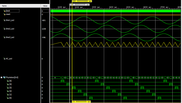 Figure7: Simulated rectified six pulses DC output for α=90º
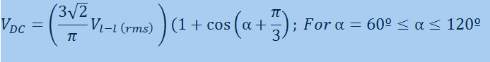
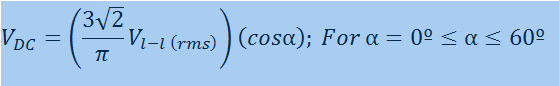
As I mentioned at the beginning of this article, there is a direct relationship between the DC output and the phase delay angle, and this is how they are related:
Controlled rectifier with free wheeling diode:
Conclusion: This AC-DC converter design did not have to be implemented on an FPGA at all, it could have been implemented on a TI DSP processor or any other similar processor. It was just the need of my application that I had to use an FPGA as I have other peripherals and modules in my system that needed intensive computations within short amount of time. I plan in the future to demo this project in this website on a TI C2000 processor. Check back!
Author: Farid M, https://embeddeddesign.org/
If you find any of the projects posted here helpful to you while working on similar projects, or you learned something from any of the topics discussed, please do not hesitate to make a donation, whatever amount you can afford, just as a gesture of appreciation and to keep this website alive and progressing so that its benefits extends to many younger engineers and students around the globe

I see you don’t monetize embeddeddesign.org, don’t waste your traffic, you can earn extra bucks every month with new monetization method.
This is the best adsense alternative for any type of website (they
approve all sites), for more details simply search in gooogle: murgrabia’s tools
LikeLike
My only intention from writing in this website is to share knowledge. It’s not meant for generating income!
LikeLike
My only intention for launching this website is to promote knowledge. It is not for generating income.
LikeLike
Please add the source: Author: Farid M, https://embeddeddesign.org/
LikeLike
Please add the source: Author: Farid M, https://embeddeddesign.org/
LikeLike
Please add the source: Author: Farid M, https://embeddeddesign.org/
LikeLike
Can you please provide the pic18 program for PWM generation for 3 phase full wave controlled rectifier
LikeLike