
This post is to how you how to configure an SPI on STM32F4 and use it to interface with an ADC. As an example, I am using MCP3204T, which is a 12 bits ADC from Microchip with four channels. The source code runs on STM32F4 Discovery board, and it was tested with actual real life measurements. In the mean time, I have to mention that both the STM32F4 MCU and ADC are great for industrial applications.
Figure1. STM32F407 Discovery Board
Before I move into how the code is configured and how it works. I would like to start off by an brief explanation about how the SPI protocol works.
SPI is a serial communication protocol and it stands for Serial Peripheral Interface. It was developed by Motorola in mid 1980s. It is also referred to as four-wire bus, as it has four wire: MISO (Master Input Slave Output), MOSI (Master Output Slave Input), CS Chip Select), and CLK( clock.) The clock speed on STM32F4 can run up to 10MHz. It is the master that controls the clock and initiates transactions by pulling the CS signal low. The master can address multiple slaves, but it can communicate only with one slave at a time. Data from master is sent through MOSI line and data from slaves is received through MISO line.
 Figure1. Master configuration with three independent slaves[1]
Besides setting up the clock frequency, the master also has to configure the clock polarity and phase with respect to the data. These are named CPOL and CPHA.
 Figure2. Timing diagram showing clock polarity and phase[1]
CPOL=0 means the leading edge is a rising edge, and the trailing edge is a falling edge. CPOL=1 denotes The leading edge is a falling edge, and the trailing edge is a rising edge.
In total there are four mode:
Mode0: in this mode CPOL=0 and CPHA=0; here data is sampled at the leading rising edge of the clock. Mode 0 is the most common mode for SPI communication.
Mode1: in this mode CPOL=0 and CPHA=1, and data is sampled on the trailing falling edge.
Mode2: in this mode CPOL=1 and CPHA=0, and data is sampled on the leading falling edge.
Mode3: in this mode CPOL=1 and CPHA=1, and data is sampled on the trailing rising edge.
Firmware Implementation
The firmware for this project is at my Github respository: MCP3204T-ADC-SPI. Looking at the datasheet of the ADC MCP3904T, page 18, we can see that this ADC uses mode 0 for clock polarity and phase. This 12 bits ADC send data as a 24 bits, in three bytes starting with the most significant bit, MSB. The MCU sends a request to read a certain ADC channel by sending a start bit, followed by a bit that defines if the ADC configuration is single ended or differential, followed by three bits for the channel address starting with the MSB bit: see table below as well for address configuration.
 Figure3. SPI Communication using 8-bit segments (Mode 0,0: CLK idles low)[2]
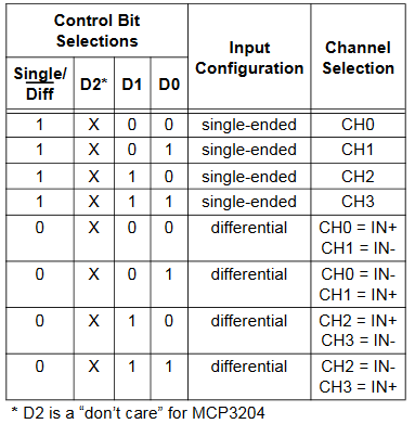
Figure4. ADC channels address bits configuration[2]
SPI Firmware Configuration
void SPI3_Config(void)
{
Spi3Handle.Instance = SPI3;
Spi3Handle.Init.Mode = SPI_MODE_MASTER;
Spi3Handle.Instance = SPI3;
Spi3Handle.Init.BaudRatePrescaler = SPI_BAUDRATEPRESCALER_256; // 42MHz/256=167kHz < 400kHz
Spi3Handle.Init.Direction = SPI_DIRECTION_2LINES;
Spi3Handle.Init.CLKPhase = SPI_PHASE_1EDGE;
Spi3Handle.Init.CLKPolarity = SPI_POLARITY_LOW;
Spi3Handle.Init.CRCCalculation = SPI_CRCCALCULATION_DISABLED;
Spi3Handle.Init.CRCPolynomial = 7;
Spi3Handle.Init.DataSize = SPI_DATASIZE_8BIT;
Spi3Handle.Init.FirstBit = SPI_FIRSTBIT_MSB;
Spi3Handle.Init.NSS = SPI_NSS_HARD_OUTPUT;
Spi3Handle.Init.TIMode = SPI_TIMODE_DISABLED;

if(HAL_SPI_Init(&Spi3Handle) != HAL_OK)
{
/* Initialization Error */
SPI3Error_Handler();
}

}
GPIO configuration:
void HAL_SPI_MspInit(SPI_HandleTypeDef *hspi)
{
GPIO_InitTypeDef GPIO_InitStruct;

/* Enable SPI clock */
__SPI3_CLK_ENABLE();

/* Enable GPIOs clock */
__GPIOC_CLK_ENABLE();

/* SPI3 SCK GPIO pin configuration */
GPIO_InitStruct.Pin = SPI3_SCK_PIN;
GPIO_InitStruct.Mode = GPIO_MODE_AF_PP;
GPIO_InitStruct.Pull = GPIO_PULLUP;
GPIO_InitStruct.Speed = GPIO_SPEED_FAST;
GPIO_InitStruct.Alternate = SPI3_SCK_AF;

HAL_GPIO_Init(SPI3_SCK_GPIO_PORT, &GPIO_InitStruct);

/* SPI3 MISO GPIO pin configuration */
GPIO_InitStruct.Pin = SPI3_MISO_PIN;
GPIO_InitStruct.Alternate = SPI3_MISO_AF;
HAL_GPIO_Init(SPI3_MISO_GPIO_PORT, &GPIO_InitStruct);

/* SPI3 MOSI GPIO pin configuration */
GPIO_InitStruct.Pin = SPI3_MOSI_PIN;
GPIO_InitStruct.Alternate = SPI3_MOSI_AF;
HAL_GPIO_Init(SPI3_MOSI_GPIO_PORT, &GPIO_InitStruct);
}
ADC channels readings: ADC data is read every 500ms. This time interval is generated with a timer interrupt. Notice in the interrupt service routine below that I just a flag to signal to the main loop that it is time to read an ADC channel. It is very critical to make your service routine as short as possible.
/**
* @brief This function handles timer2 interrupt.
*/
void HAL_TIM_PeriodElapsedCallback(TIM_HandleTypeDef *Tim2Handle)
{
  if(ADC_SampleFlag==false)                     //this flag is turned off by main while loop once data is read from ADC
  {
    ADC_SampleFlag=true;                       //notify main loop that data needs to be sampled
  }

}
And inside this while loop where the ADC read function is called.
/*wait for interrupts*/
  while (1)
  {
   if(ADC_SampleFlag==true)                     //this flag is turned ON by timer interrupt to signal it's time to read data from ADC
   {
     HAL_GPIO_TogglePin(GPIOD,GPIO_PIN_12);     //toggle an LED jsut for testing/debugging
     ADC_SampleFlag=true;                       //notify main loop that data needs to be sampled
     MCP3204_ReadRequest(counter);              // Read Channel 0
     ADC_SampleFlag=false;
     ChannelAddr++;
        if(ChannelAddr==0x04)
        {
	  ChannelAddrr=0;
        }
      }
  }
The ADC read function definition is defined below. For more understanding on the data sequence to be sent via the SPI, read page 15 and page 18 of: https://ww1.microchip.com/downloads/en/DeviceDoc/21298c.pdf
void MCP3204_ReadRequest(uint8_t address)
{
//Read page 15 and page 18 of: https://ww1.microchip.com/downloads/en/DeviceDoc/21298c.pdf
uint8_t RegisterAddressBuff1[3]={0};

RegisterAddressBuff1[0]=0x06;
RegisterAddressBuff1[1]= address<<6;
RegisterAddressBuff1[2]=0;

HAL_GPIO_WritePin(GPIOE, SPI3_CS, GPIO_PIN_RESET);

while (HAL_SPI_GetState(&Spi3Handle) != HAL_SPI_STATE_READY){}

if(address==0x00)
{
HAL_SPI_TransmitReceive(&Spi3Handle, &RegisterAddressBuff1[0], &ADC_Ch0[0],3, 1000);
}
else if(address==0x01)
{
HAL_SPI_TransmitReceive(&Spi3Handle, &RegisterAddressBuff1[0], &ADC_Ch1[0],3, 1000);
}
else if(address==0x02)
{
HAL_SPI_TransmitReceive(&Spi3Handle, &RegisterAddressBuff1[0], &ADC_Ch2[0],3, 1000);
}
else if(address==0x03)
{
HAL_SPI_TransmitReceive(&Spi3Handle, &RegisterAddressBuff1[0], &ADC_Ch3[0],3, 1000);
}
HAL_GPIO_WritePin(GPIOE, SPI3_CS, GPIO_PIN_SET);
}
Measurements Results
The plots on the scope below shows the SPI signals: Blue signal is Chip Select line, Purple color signal is MOSI signal ( MCU data request/master data), Green signal is MISO(the ADC readings/slave data), and the yellow color signal is the is the SPI clock. Since the master sends 24 bits, it means twenty four clock cycles needs to be generated. The coursers show the time taken to send 24 bits. From this time measurements we can verify the clock speed that we selected in the configuration above: clock frequency=1/(147/24)=163.043 KHz. But in fact the precise the SPI clock frequency is 167KHz. The slight difference in values is just due the low resolution I have on my scope when I took the screen shot.
The MISO line shows the ADC readings for channel 2: 0x7D0 hex, 2000 Dec . This converts to an analog reading of: (2000/4095)*3=1.465V.
 Figure5. SPI Signals: CS in blue, SCLK in yellow, MOSI in purple, MISO in green
If you find any of the projects posted here helpful to you while working on similar projects, or you learned something from any of the topics discussed, please do not hesitate to make a donation, whatever amount you can afford, just as a gesture of appreciation and to keep this website alive and progressing so that its benefits extends to many younger engineers and students around the globe
References
[1] “Serial Peripheral Interface.” Retrieved from https://en.wikipedia.org/wiki/Serial_Peripheral_Interface#/media/File:SPI_timing_diagram2.svg
[2] “2.7V 4-Channel/8-Channel 12-Bit A/D Converters with SPI Serial Interface.” Retrieved from https://ww1.microchip.com/downloads/en/DeviceDoc/21298c.pdf
