
Author: Farid M, https://embeddeddesign.org/
In my previous posting, I talked in details about the implementation of peak current mode control for a single phase synchronous DC-DC buck converter. In this article, I would like to share with you the firmware implementation of peak current mode control loop for a multi-phase synchronous buck converter.
You might be asking why not a single phase instead of multi-phase, as latter will only make the design more complex and add just more cost to the bill of material, PCB layout and manufacturing. To answer this question, I will start off my discussion by listing the benefits of a multi-phase buck converter:
- In a single stage power dissipation is high at high currents above 25A, and optimizing design for higher efficiency at this level of current can be challenging[1].
- Output filter requirements in a multi-stage system are less than in a single stage, and this is due to the fact that each stage require lesser current flow[1].
- Multi-stage converters has output current ripples cancellation which means less ripples on the output unlike single stage DC-DC converters[1].
- Current ripples cancellations results in minimal overshoot and undershoot[1].
- Load transient performance in better in multi-stage than in single stage and this is due to the fact that lesser energy are stored in the inductors.
- Multistage buck converters required lesser input capacitance. “adding additional phases to a design decreases the RMS input current flowing through the decoupling capacitors thereby reducing the ripple on the input voltage. Fewer capacitors are then needed to keep input voltage ripple within specifications. Self-heating effects within the capacitors themselves due to equivalent series resistance,ESR,are also reduced“[2].
- Lesser input and output capacitance requirements, as well as lesser current flow in each stage means better thermal performance than signal stage converters.
Firmware Implementation
All the discussions coming up are related to Biricha TI application note[3]. It is assumed that the reader has sufficient knowledge about buck converters design, control theory in general and peak current mode control theory in particular. However, if the reader needs to refresh their memory or get familiar with DC-DC buck converters designs and peak current mode control theory, these links[3] and [4] are very useful.
The firmware for this multistage DC-DC buck converter was implemented on a TI C2000 Picolo DSP MCU: MTS320F2869, and it was tested with this MCU development board, MCU F28069M LaunchPad: https://amzn.to/2SRTyf8, and a digital power buck converter board:BOOSTXL-BUCKCONV.
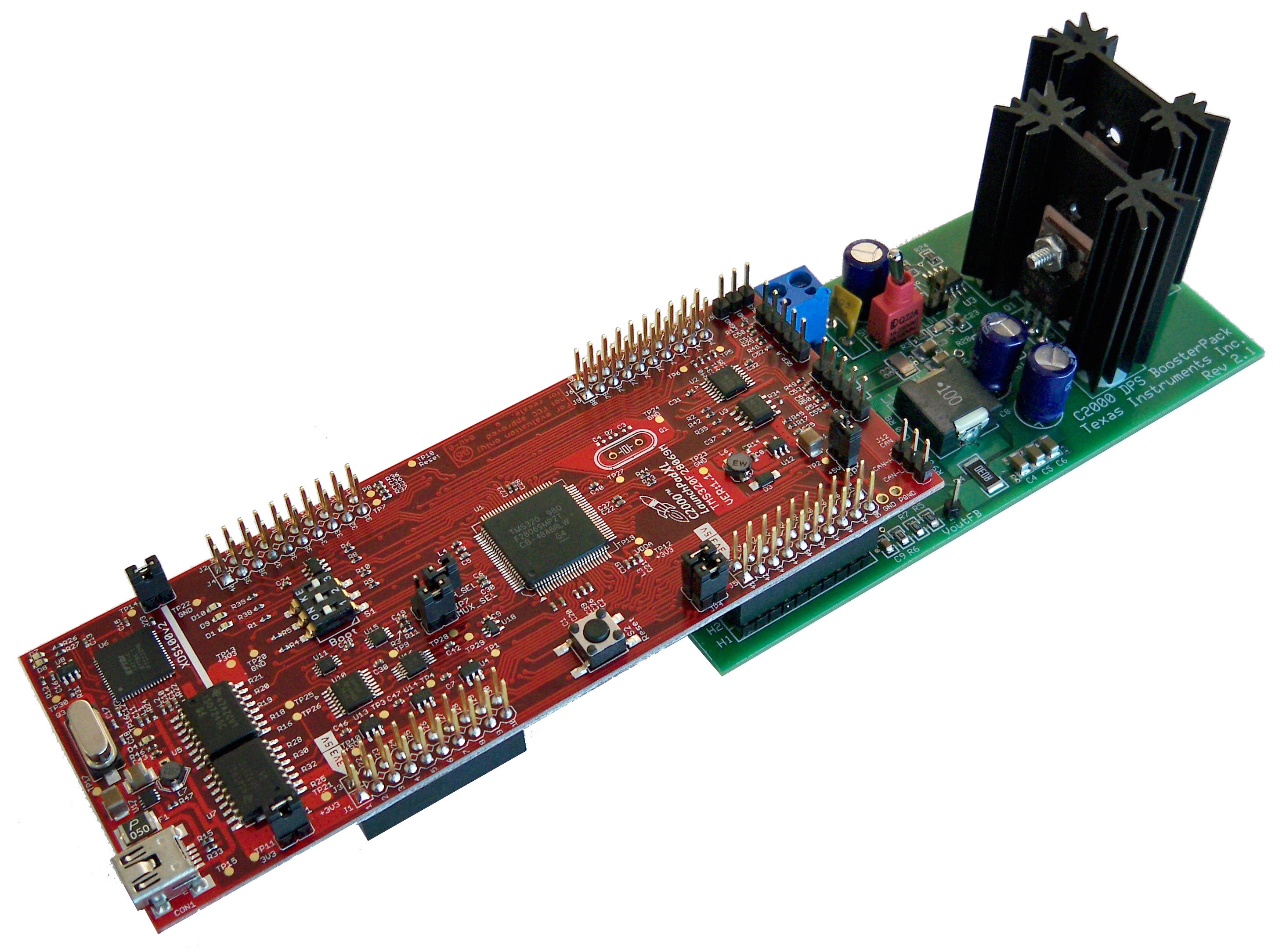 Figure2. MCU F28069M LaunchPad and Digital Power Buck Converter Board
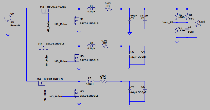
The design requirement of this project is to generate a +4VDC output voltage that can delivers up to 6A output current. The system is supposed to be stable with a phase margin of at least 45 degrees, and it has to have a crossover frequency equal to 15KHz.
Peripheral Requirements
- I needed 6 PWMs to drive the six MOSFETS: M1-M6. I used PWM3A switches M2, PWM3B switches M1 in the first power stage. PWM4A switches M4, and PWM4B switches M3 in the second stage. PWM5A switches M6, and PWM5B switches M5 in the third stage. The switching frequency was selected to be equal to 200KHz.
- All six PWMs make 3 pairs: 2 PWMs (Channel A and B) per power stage, and each pair have a 120 degrees phase shift (about1.67us.)Meaning that each power stage have a phase shift of 120 degrees. Each pair of PWMs are complimentary and they use the bad gap submodule so that each pair of MOSFETs can’t be turned on at the same time.
- PWM1B, PWM2B and PWM6B were used to trigger the ADC start of conversion, SOC. PWM1B triggers ADC conversion for the analog output of first stage, PWM2B triggers ADC conversion for the analog output of second stage,and PWM6B triggers ADC conversion for the analog output of the third stage.
- Upon an ADC end of conversion, EOC, a CLA task is triggered. Thus, in total I had to use three CLA tasks to process the closed control loop: one task per control loop. This also meant I had to use three ADC channels.
- I used three analog comparators: COMP1, COMP2, and COMP3. Comparator1 trips PWM3A when its DC output goes high, and Comparator2 trips PWM4A when its output goes high, and comparator3 trips PWM5A when its DC output goes high. Note here that the non inverting pin of each comparator is connected to inductor current sensor and the inverting pin is connected to the internal DAC (all three DACs are used).
- PWM1A is used as a master for all PWMs. All phases are in reference to PWMA.
- Internal DAC slope compensation was used in all three stages as our duty cycle in this design is near 50%.
Hardware Configuration
The coming up paragraphs give details for the hardware configuration of each subsystem mentioned above. The source code file can be downloaded from Github
ADC: there three ADC Channels and they are configured as below. Three start of conversions, SOC0, SOC1 and SOC3 are used for one ADC channel: ADCINB0. SOC0, SOC1 and SOC3 are triggered by EPWM1B, EPWM2B, and EPWM6B, respectively. End of Conversion EOC0, EOC1, EOC2 are setup to trigger ADCINT1, ADCINT2, and ADCINT3 to fire, and consequently triggers CLA task1, task2 and task3.
EALLOW;
AdcRegs.INTSEL1N2.bit.INT1E = 1;         /* Enabled ADCINT1 */
AdcRegs.INTSEL1N2.bit.INT1CONT = 0;      /* Disable ADCINT1 Continuous mode */
AdcRegs.INTSEL1N2.bit.INT1SEL = 0;       /* setup EOC0 to trigger ADCINT1 to fire */
AdcRegs.ADCSOC0CTL.bit.CHSEL = 0x3;      /* Set SOC0 channel select to ADCINB0 */
AdcRegs.ADCSOC0CTL.bit.TRIGSEL = ADCTRIG_EPWM1_SOCB; /* Set SOC0 start trigger on EPWM1B, due to round-robin SOC0 converts first then SOC1 */
AdcRegs.ADCSOC0CTL.bit.ACQPS = 6;       /* Set SOC0 S/H Window to 7 ADC Clock Cycles, (6 ACQPS plus 1) */
AdcRegs.ADCCTL1.bit.INTPULSEPOS = 0;    /* Configure early interrupts */
EDIS;

EALLOW;
AdcRegs.INTSEL1N2.bit.INT2E = 1; /* Enabled ADCINT2 */
AdcRegs.INTSEL1N2.bit.INT2CONT = 0; /* Disable ADCINT2 Continuous mode */
AdcRegs.INTSEL1N2.bit.INT2SEL = 1; /* setup EOC1 to trigger ADCINT2 to fire */
AdcRegs.ADCSOC1CTL.bit.CHSEL = 0x3; /* Set SOC1 channel select to ADCINB0 */
AdcRegs.ADCSOC1CTL.bit.TRIGSEL = ADCTRIG_EPWM2_SOCB; /* Set SOC1 start trigger on EPWM2A, due to round-robin SOC1 converts first then SOC1 */
AdcRegs.ADCSOC1CTL.bit.ACQPS = 6; /* Set SOC0 S/H Window to 7 ADC Clock Cycles, (6 ACQPS plus 1) */
AdcRegs.ADCCTL1.bit.INTPULSEPOS = 0; /* Configure early interrupts */
EDIS;

EALLOW;
AdcRegs.INTSEL3N4.bit.INT3E = 1;      /* Enabled ADCINT3 */
AdcRegs.INTSEL3N4.bit.INT3CONT = 0;   /* Disable ADCINT3 Continuous mode */
AdcRegs.INTSEL3N4.bit.INT3SEL = 2;    /* setup EOC2 to trigger ADCINT3 to fire */
AdcRegs.ADCSOC2CTL.bit.CHSEL = 0x3;   /* Set SOC2 channel select to ADCINB0*/
AdcRegs.ADCSOC2CTL.bit.TRIGSEL= ADCTRIG_EPWM6_SOCB; /* Set SOC2 start trigger on EPWM6B, due to round-robin SOC2 converts first then SOC2 */
AdcRegs.ADCSOC2CTL.bit.ACQPS = 6;    /* Set SOC2 S/H Window to 7 ADC Clock Cycles, (6 ACQPS plus 1) */
AdcRegs.ADCCTL1.bit.INTPULSEPOS = 0; /* Configure early interrupts */
EDIS;
Comparators: The system uses three internal analog comparators: COMP1, COMP2, and COMP3. The non-inverting of each comparator is connected to the internal DAC, which generates an analog signal for the output of the PID or 2P2Z controller. The inverting pin is connected to inductor current sensor. When the inductor current goes above the DAC DC signal, the output of the comparator goes high and trips the PWM signal that swithes the inductor.
/* Configure Comparator 1: link cmp1 to pwm3*/
EALLOW;
SysCtrlRegs.PCLKCR3.bit.COMP1ENCLK = 1;
Comp1Regs.COMPCTL.bit.COMPDACEN = 1;             // Power up Comparator locally
Comp1Regs.COMPCTL.bit.COMPSOURCE = 0;            // Connect the inverting input to internal DAC
Comp1Regs.DACCTL.bit.DACSOURCE = 1;              // 0 - DACVAL; 1 - Internal ramp for slope compensation
Comp1Regs.COMPCTL.bit.QUALSEL = 5;               // Comparator output must be active for 4 consecutive clocks before resetting the RAMP
Comp1Regs.DACCTL.bit.RAMPSOURCE = 2;             // 0 - PMW1; 1 - PWM2, 2 -PWM3  4-PWM5 ...so on
Comp1Regs.RAMPDECVAL_SHDW = slopeval;
EPwm1Regs.HRPCTL.bit.PWMSYNCSEL = 1;             // PWM SYNC generated at CTR = ZRO for synchronizing internal ramp
Comp1Regs.COMPCTL.bit.CMPINV = 0;                // Comparator Output passed
EDIS;

/* Configure Comparator 2: link cmp2 to pwm4*/
EALLOW;
SysCtrlRegs.PCLKCR3.bit.COMP2ENCLK = 1;
Comp2Regs.COMPCTL.bit.COMPDACEN = 1;             // Power up Comparator locally
Comp2Regs.COMPCTL.bit.COMPSOURCE = 0;            // Connect the inverting input to internal DAC
Comp2Regs.DACCTL.bit.DACSOURCE = 1;              // 0 - DACVAL; 1 - Internal ramp for slope compensation
Comp2Regs.COMPCTL.bit.QUALSEL = 5;               // Comparator output must be active for 4 consecutive clocks before resetting the RAMP
Comp2Regs.DACCTL.bit.RAMPSOURCE = 3;             // 0 - PMW1; 1 - PWM2, 3- PWM4 ...so on link cmp2 to pwm4
Comp2Regs.RAMPDECVAL_SHDW = slopeval;
EPwm2Regs.HRPCTL.bit.PWMSYNCSEL = 1;             // PWM SYNC generated at CTR = ZRO for synchronizing internal ramp
Comp2Regs.COMPCTL.bit.CMPINV = 0;                // Comparator Output passed
EDIS;

/* Configure Comparator 3: link cmp1 to pwm5 */
EALLOW;
SysCtrlRegs.PCLKCR3.bit.COMP3ENCLK = 1;
Comp3Regs.COMPCTL.bit.COMPDACEN = 1;             // Power up Comparator locally
Comp3Regs.COMPCTL.bit.COMPSOURCE = 0;            // Connect the inverting input to internal DAC
Comp3Regs.DACCTL.bit.DACSOURCE = 1;              // 0 - DACVAL; 1 - Internal ramp for slope compensation
Comp3Regs.COMPCTL.bit.QUALSEL = 5;               // Comparator output must be active for 4 consecutive clocks before resetting the RAMP
Comp3Regs.DACCTL.bit.RAMPSOURCE = 4;             // 0 - PMW1; 1 - PWM2, 5- PWM6 ...so on
Comp3Regs.RAMPDECVAL_SHDW = slopeval;
EPwm3Regs.HRPCTL.bit.PWMSYNCSEL = 1;             // PWM SYNC generated at CTR = ZRO for synchronizing internal ramp
Comp3Regs.COMPCTL.bit.CMPINV = 0;                // Comparator Output passed
EDIS;
EPWMs: EPWM1A is set up as a master, and the rest of PWMs are configured as slaves. EPWM3A and EPWM2B are complimentary with a band gap of 15 clock cycles. They control the first power phase. EPWM4A and EPWM4B are also complimentary with a band gap of 15 clock cycles, and they control the second power phase. EPWM5A and EPWM5B are also complimentary with a band gap of 15 clock cycles, and they control the first power phase. In total, I have three pairs of EPWMs: one pair per power phase, and each of these pair are 120 degrees out of phase with each other, 1.67us for a 200KHz frequency.
void PWMs_Config(void)
{
  /* Configure PWMs */
   EALLOW;
   /* Assumes ePWM1 clock is already enabled in InitSysCtrl(); */
   EPwm1Regs.ETSEL.bit.SOCBEN = 1;        /* Enable SOC on B group */
   EPwm1Regs.ETSEL.bit.SOCBSEL = 6;       /* Select SOC from from CPMB on upcount */
   EPwm1Regs.ETPS.bit.SOCBPRD = 1;        /* Generate pulse on 1st event */
   /* Set period / duty / count mode */
   EPwm1Regs.TBPHS.half.TBPHS = 0;             /* Set Phase register to zero */
   EPwm1Regs.TBCTL.bit.PHSEN = TB_DISABLE;     /* Phase loading disabled */
   EPwm1Regs.TBCTL.bit.HSPCLKDIV = TB_DIV1;    /* Clock ratio to SYSCLKOUT */
   EPwm1Regs.TBCTL.bit.CLKDIV = TB_DIV1;
   EPwm1Regs.TBCTL.bit.PRDLD = TB_SHADOW;
   EPwm1Regs.AQCTLA.bit.ZRO = AQ_SET;          /* Set PWM1A on Zero */
   EPwm1Regs.AQCTLA.bit.CAU = AQ_CLEAR;        /* Clear PWM1A on match on count A up */
   EPwm1Regs.AQCTLB.bit.ZRO = AQ_SET;          /* Set PWM1B on Zero */
   EPwm1Regs.AQCTLB.bit.CBU = AQ_CLEAR;        /* Clear PWM1B on match on count B up */
   EPwm1Regs.CMPB = DutyCycle_PWMB;                       /* Set compare B value */
   EPwm1Regs.CMPA.half.CMPA = DutyCycle_PWMA;             /* Set compare A value */
   EPwm1Regs.TBPRD = PERIOD;                   /* Set period for ePWM1 */
   EPwm1Regs.TBCTL.bit.CTRMODE = TB_COUNT_UP;  /* Count up and start */
   EPwm1Regs.CMPCTL.bit.SHDWAMODE = CC_SHADOW;
   EPwm1Regs.CMPCTL.bit.LOADAMODE = CC_CTR_PRD;
   EPwm1Regs.TBCTL.bit.SYNCOSEL = TB_CTR_ZERO; // sync "down-stream"
   EDIS;
   /* Assumes ePWM2 clock is already enabled in InitSysCtrl(); */
   EALLOW;
   EPwm2Regs.ETSEL.bit.SOCBEN = 1;        /* Enable SOC on B group */
   EPwm2Regs.ETSEL.bit.SOCBSEL = 6;       /* Select SOC from from CPMB on upcount */
   EPwm2Regs.ETPS.bit.SOCBPRD = 1;        /* Generate pulse on 1st event */
   /* Set period / duty / count mode */
   EPwm2Regs.TBPHS.half.TBPHS = PHASE1;             /* Set Phase register to zero */
   EPwm2Regs.TBCTL.bit.PHSEN = TB_ENABLE;           /* Phase loading disabled */
   EPwm2Regs.TBCTL.bit.HSPCLKDIV = TB_DIV1;         /* Clock ratio to SYSCLKOUT */
   EPwm2Regs.TBCTL.bit.CLKDIV = TB_DIV1;
   EPwm2Regs.TBCTL.bit.PRDLD = TB_SHADOW;
   EPwm2Regs.AQCTLA.bit.ZRO = AQ_SET;          /* Set PWM2A on Zero */
   EPwm2Regs.AQCTLA.bit.CAU = AQ_CLEAR;        /* Clear PWM2A on match on count A up */
   EPwm2Regs.AQCTLB.bit.ZRO = AQ_SET;          /* Set PWM1B on Zero */
   EPwm2Regs.AQCTLB.bit.CBU = AQ_CLEAR;        /* Clear PWM1B on match on count B up */
   EPwm2Regs.CMPB = DutyCycle_PWMB;                       /* Set compare B value */
   EPwm2Regs.CMPA.half.CMPA = DutyCycle_PWMA;             /* Set compare A value */
   EPwm2Regs.TBPRD = PERIOD;                   /* Set period for ePWM1 */
   EPwm2Regs.TBCTL.bit.CTRMODE = TB_COUNT_UP;  /* Count up and start */
   EPwm2Regs.CMPCTL.bit.SHDWAMODE = CC_SHADOW;
   EPwm2Regs.CMPCTL.bit.LOADAMODE = CC_CTR_PRD;
   EPwm2Regs.TBCTL.bit.SYNCOSEL = TB_SYNC_IN; // sync "down-stream"
   EDIS;

   EALLOW;
   EPwm6Regs.ETSEL.bit.SOCBEN = 1;        /* Enable SOC on B group */
   EPwm6Regs.ETSEL.bit.SOCBSEL = 6;       /* Select SOC from from CPMB on upcount */
   EPwm6Regs.ETPS.bit.SOCBPRD = 1;        /* Generate pulse on 1st event */
   /*PWM6: Set period / duty / count mode */
   EPwm6Regs.TBPHS.half.TBPHS = PHASE2;             /* Set Phase register to zero */
   EPwm6Regs.TBCTL.bit.PHSEN = TB_ENABLE;           /* Phase loading disabled */
   EPwm6Regs.TBCTL.bit.HSPCLKDIV = TB_DIV1;         /* Clock ratio to SYSCLKOUT */
   EPwm6Regs.TBCTL.bit.CLKDIV = TB_DIV1;
   EPwm6Regs.TBCTL.bit.PRDLD = TB_SHADOW;
   EPwm6Regs.AQCTLA.bit.ZRO = AQ_SET;          /* Set PWM1A on Zero */
   EPwm6Regs.AQCTLA.bit.CAU = AQ_CLEAR;        /* Clear PWM6A on match on count A up */
   EPwm6Regs.AQCTLB.bit.ZRO = AQ_SET;          /* Set PWM6B on Zero */
   EPwm6Regs.AQCTLB.bit.CBU = AQ_CLEAR;        /* Clear PWM6B on match on count B up */
   EPwm6Regs.CMPB = DutyCycle_PWMB;                         /* Set compare B value */
   EPwm6Regs.CMPA.half.CMPA = DutyCycle_PWMA;               /* Set compare A value */
   EPwm6Regs.TBPRD = PERIOD;                                /* Set period for ePWM1 */
   EPwm6Regs.TBCTL.bit.CTRMODE = TB_COUNT_UP;               /* Count up and start */
   EPwm6Regs.CMPCTL.bit.SHDWAMODE = CC_SHADOW;
   EPwm6Regs.CMPCTL.bit.LOADAMODE = CC_CTR_PRD;
   EPwm6Regs.TBCTL.bit.SYNCOSEL = TB_SYNC_IN;              // sync "down-stream"
   EDIS;

   EALLOW;
   /*PWM3: Set period / duty / count mode */
   EPwm3Regs.TBPHS.half.TBPHS = 0;             /* Set Phase register to zero */
   EPwm3Regs.TBCTL.bit.PHSEN = TB_ENABLE;      /* Phase loading disabled */
   EPwm3Regs.TBCTL.bit.HSPCLKDIV = TB_DIV1;    /* Clock ratio to SYSCLKOUT */
   EPwm3Regs.TBCTL.bit.CLKDIV = TB_DIV1;
   EPwm3Regs.TBCTL.bit.PRDLD = TB_SHADOW;
   EPwm3Regs.AQCTLA.bit.ZRO = AQ_SET;          /* Set PWM3A on Zero */
   EPwm3Regs.AQCTLA.bit.CAU = AQ_CLEAR;        /* Clear PWM3A on match on count A up */
   EPwm3Regs.AQCTLB.bit.ZRO = AQ_SET;          /* Set PWM3B on Zero */
   EPwm3Regs.AQCTLB.bit.CBU = AQ_CLEAR;        /* Clear PWM3B on match on count B up */
   EPwm3Regs.CMPA.half.CMPA =DutyCycle_PWMA;             /* Set compare A value */
   EPwm3Regs.TBPRD = PERIOD;                             /* Set period for ePWM3 */
   EPwm3Regs.TBCTL.bit.CTRMODE = TB_COUNT_UPDOWN; //TB_COUNT_UP;            /* Count up and start */
   EPwm3Regs.CMPCTL.bit.SHDWAMODE = CC_SHADOW;
   EPwm3Regs.CMPCTL.bit.SHDWBMODE = CC_SHADOW;
   EPwm3Regs.CMPCTL.bit.LOADAMODE =  CC_CTR_PRD;
   EPwm3Regs.CMPCTL.bit.LOADBMODE =  CC_CTR_PRD;
   EPwm3Regs.TBCTL.bit.SYNCOSEL = TB_SYNC_IN;           // sync "down-stream" slave
   EDIS;
   /* Configure trip zone based on Comparator 3 output and configure blanking */
   EALLOW;
   EPwm3Regs.TZSEL.bit.DCAEVT2 = 1;                      // Disable DCAEVT2 as a CBC trip source for this ePWM module /* Digital compare, output A, cycle by cycle */
   EPwm3Regs.TZCTL.bit.TZA = TZ_FORCE_LO;                /* EPWM3A will go low */
   EPwm3Regs.TZCTL.bit.TZB = TZ_FORCE_HI;                /* EPWM3B goes HI */
   EPwm3Regs.DCTRIPSEL.bit.DCAHCOMPSEL = DC_COMP1OUT;    // DCAH = Comparator 1 output
   EPwm3Regs.TZDCSEL.bit.DCAEVT2 = TZ_DCAH_HI;           /* DCAEVT2 =  DCAL High (will become active as Comparator output goes High) */
                                                         /* DCAEVT2 = DCAH high (will become EPwm1Regs.DCTRIPSEL.bit.DCAHCOMPSEL = DC_COMP2OUT; DCAH = Comparator 2 output*/
   EPwm3Regs.DCACTL.bit.EVT2SRCSEL = DC_EVT2;            /* DCAEVT2 = DCAEVT2 (not filtered) */
   EPwm3Regs.DCACTL.bit.EVT2FRCSYNCSEL = DC_EVT_ASYNC;   /* Take async path */
   EPwm3Regs.DCFCTL.bit.PULSESEL = 0;                    /* Time-base counter equal to period (TBCTR =TBPRD) */
   EPwm3Regs.DCFCTL.bit.BLANKINV = 0;                    /* Blanking window inverted */
   EPwm3Regs.DCFCTL.bit.BLANKE = 1;                      /* Blanking Window Enable */
   EPwm3Regs.DCFCTL.bit.SRCSEL = 0;                      /* Source Is DCAEVT1 Signal */
   EPwm3Regs.DCFWINDOW = 0; //34;                        /* length blanking window: this corresponds to: 34*11.1ns=377.4ns*/
   EPwm3Regs.DCFOFFSET = 5;                              /* 5*11.1=55.5ns blanking window offset & then blanking window begins */
   // Active high complementary PWMs - Set up the deadband
   EPwm3Regs.DBCTL.bit.IN_MODE = DBA_ALL;
   EPwm3Regs.DBCTL.bit.OUT_MODE = DB_FULL_ENABLE;
   EPwm3Regs.DBCTL.bit.POLSEL = DB_ACTV_HIC;
   EPwm3Regs.DBRED = 15;
   EPwm3Regs.DBFED = 15;
   EDIS;
   /* Assumes ePWM4 clock is already enabled in InitSysCtrl(); */
   EALLOW;
   /*PWM4: Set period / duty / count mode */
   EPwm4Regs.TBPHS.half.TBPHS = PHASE1;             /* Set Phase register to zero */
   EPwm4Regs.TBCTL.bit.PHSEN = TB_ENABLE;           /* Phase loading disabled */
   EPwm4Regs.TBCTL.bit.HSPCLKDIV = TB_DIV1;         /* Clock ratio to SYSCLKOUT */
   EPwm4Regs.TBCTL.bit.CLKDIV = TB_DIV1;
   EPwm4Regs.TBCTL.bit.PRDLD = TB_SHADOW;
   EPwm4Regs.AQCTLA.bit.ZRO = AQ_SET;          /* Set PWM4A on Zero */
   EPwm4Regs.AQCTLA.bit.CAU = AQ_CLEAR;        /* Clear PWM4A on match on count A up */
   EPwm4Regs.AQCTLB.bit.ZRO = AQ_SET;          /* Set PWM4B on Zero */
   EPwm4Regs.AQCTLB.bit.CBU = AQ_CLEAR;        /* Clear PWM4B on match on count B up */
   EPwm4Regs.CMPA.half.CMPA =DutyCycle_PWMA;             /* Set compare A value */
   EPwm4Regs.TBPRD = PERIOD;                             /* Set period for ePWM1 */
   EPwm4Regs.TBCTL.bit.CTRMODE = TB_COUNT_UP;            /* Count up and start */
   EPwm4Regs.CMPCTL.bit.SHDWAMODE = CC_SHADOW;
   EPwm4Regs.CMPCTL.bit.LOADAMODE = CC_CTR_PRD;
   EPwm4Regs.TBCTL.bit.SYNCOSEL = TB_SYNC_IN;          // sync "down-stream" slave
   EDIS;
   /* Configure trip zone based on Comparator 2 output and configure blanking */
   EALLOW;
   EPwm4Regs.TZSEL.bit.DCAEVT2 = 1;                      /* Digital compare, output A, cycle by cycle */
   EPwm4Regs.TZCTL.bit.TZA = TZ_FORCE_LO;                /* EPWM4A will go low */
   EPwm4Regs.TZCTL.bit.TZB = TZ_FORCE_HI;                /* EPWM4B goes HI */
   EPwm4Regs.DCTRIPSEL.bit.DCAHCOMPSEL = DC_COMP2OUT;    // DCAH = Comparator 2 output
   EPwm4Regs.TZDCSEL.bit.DCAEVT2 = TZ_DCAH_HI;           /** DCAEVT2 =  DCAL High (will become active as Comparator output goes High) */
                                                          /* DCAEVT2 = DCAH high (will become EPwm1Regs.DCTRIPSEL.bit.DCAHCOMPSEL = DC_COMP2OUT; DCAH = Comparator 2 output*/
   EPwm4Regs.DCACTL.bit.EVT2SRCSEL = DC_EVT2;            /* DCAEVT2 = DCAEVT2 (not filtered) */
   EPwm4Regs.DCACTL.bit.EVT2FRCSYNCSEL = DC_EVT_ASYNC;   /* Take async path */
   EPwm4Regs.DCFCTL.bit.PULSESEL = 0;                    /* Time-base counter equal to period (TBCTR =TBPRD) */
   EPwm4Regs.DCFCTL.bit.BLANKINV = 0;                    /* Blanking window inverted */
   EPwm4Regs.DCFCTL.bit.BLANKE = 1;                      /* Blanking Window Enable */
   EPwm4Regs.DCFCTL.bit.SRCSEL = 0;                      /* Source Is DCAEVT1 Signal */
   EPwm4Regs.DCFWINDOW = 0; //34;                        /*length blanking window: this corresponds to: 34*11.1ns=377.4ns*/
   EPwm4Regs.DCFOFFSET = 5;                              /* 5*11.1=55.5ns blanking window offset & then blanking window begins */
   EDIS;
   // Active high complementary PWMs - Set up the deadband
   EPwm4Regs.DBCTL.bit.IN_MODE = DBA_ALL;
   EPwm4Regs.DBCTL.bit.OUT_MODE = DB_FULL_ENABLE;
   EPwm4Regs.DBCTL.bit.POLSEL = DB_ACTV_HIC;
   EPwm4Regs.DBRED = 15;
   EPwm4Regs.DBFED = 15;
   EALLOW;
   /*PWM5: Set period / duty / count mode */
   EPwm5Regs.TBPHS.half.TBPHS = PHASE2;             /* Set Phase register to zero */
   EPwm5Regs.TBCTL.bit.PHSEN = TB_ENABLE;      /* Phase loading disabled */
   EPwm5Regs.TBCTL.bit.HSPCLKDIV = TB_DIV1;    /* Clock ratio to SYSCLKOUT */
   EPwm5Regs.TBCTL.bit.CLKDIV = TB_DIV1;
   EPwm5Regs.TBCTL.bit.PRDLD = TB_SHADOW;
   EPwm5Regs.AQCTLA.bit.ZRO = AQ_SET;          /* Set PWM5A on Zero */
   EPwm5Regs.AQCTLA.bit.CAU = AQ_CLEAR;        /* Clear PWM5A on match on count A up */
   EPwm5Regs.AQCTLB.bit.ZRO = AQ_SET;          /* Set PWM5B on Zero */
   EPwm5Regs.AQCTLB.bit.CBU = AQ_CLEAR;        /* Clear PWM5B on match on count B up */
   EPwm5Regs.CMPA.half.CMPA =DutyCycle_PWMA;             /* Set compare A value */
   EPwm5Regs.TBPRD = PERIOD;                             /* Set period for ePWM1 */
   EPwm5Regs.TBCTL.bit.CTRMODE = TB_COUNT_UP;            /* Count up and start */
   EPwm5Regs.CMPCTL.bit.SHDWAMODE = CC_SHADOW;
   EPwm5Regs.CMPCTL.bit.LOADAMODE = CC_CTR_PRD;
   EPwm5Regs.TBCTL.bit.SYNCOSEL = TB_SYNC_IN;           // sync "down-stream"
   EDIS;
   /* Configure trip zone based on Comparator 1 output and configure blanking */
   EALLOW;
   EPwm5Regs.TZSEL.bit.DCAEVT2 = 1;                      /* Digital compare, output A, cycle by cycle */
   EPwm5Regs.TZCTL.bit.TZA = TZ_FORCE_LO;                /* EPWM5A will go low */
   EPwm5Regs.TZCTL.bit.TZB = TZ_FORCE_HI;                /* EPWM5B goes HI */
   EPwm5Regs.DCTRIPSEL.bit.DCAHCOMPSEL = DC_COMP3OUT;    // DCAH = Comparator 1 output
   EPwm5Regs.TZDCSEL.bit.DCAEVT2 = TZ_DCAH_HI;           /** DCAEVT2 =  DCAL High (will become active as Comparator output goes High) */
                                                           /* DCAEVT2 = DCAH high (will become EPwm1Regs.DCTRIPSEL.bit.DCAHCOMPSEL = DC_COMP2OUT; DCAH = Comparator 2 output*/
   EPwm5Regs.DCACTL.bit.EVT2SRCSEL = DC_EVT2;            /* DCAEVT2 = DCAEVT2 (not filtered) */
   EPwm5Regs.DCACTL.bit.EVT2FRCSYNCSEL = DC_EVT_ASYNC;   /* Take async path */
   EPwm5Regs.DCFCTL.bit.PULSESEL = 0;                    /* Time-base counter equal to period (TBCTR =TBPRD) */
   EPwm5Regs.DCFCTL.bit.BLANKINV = 0;                    /* Blanking window inverted */
   EPwm5Regs.DCFCTL.bit.BLANKE = 1;                      /* Blanking Window Enable */
   EPwm5Regs.DCFCTL.bit.SRCSEL = 0;                      /* Source Is DCAEVT1 Signal */
   EPwm5Regs.DCFWINDOW = 0; //34;                        /*length blanking window: this corresponds to: 34*11.1ns=377.4ns*/
   EPwm5Regs.DCFOFFSET = 5;                              /* 5*11.1=55.5ns blanking window offset & then blanking window begins */
   EDIS;
   // Active high complementary PWMs - Set up the deadband
   EPwm5Regs.DBCTL.bit.IN_MODE = DBA_ALL;
   EPwm5Regs.DBCTL.bit.OUT_MODE = DB_FULL_ENABLE;
   EPwm5Regs.DBCTL.bit.POLSEL = DB_ACTV_HIC;
   EPwm5Regs.DBRED =15;
   EPwm5Regs.DBFED =15;
}
Author: Farid M, https://embeddeddesign.org/
If you find any of the projects posted here helpful to you while working on similar projects, or you learned something from any of the topics discussed, please do not hesitate to make a donation, whatever amount you can afford, just as a gesture of appreciation and to keep this website alive and progressing so that its benefits extends to many younger engineers and students around the globe.
References
[1] David, Baba. Benefits of a multiphase buck converter. PDF 2012. http://www.ti.com/lit/an/slyt449/slyt449.pdf
[2] Carmen, Parisi. Multiphase Buck Design From Start to Finish.PDF 2017. http://www.ti.com/lit/an/slva882/slva882.pdf
[3] Richard, Poley and Ali, Shirsavar. Digital Peak Current Mode Control With Slope Compensation Using the TMS320F2803x. PDF April 212.
[4] Brigitte, Hauke. Basic Calculation of a Buck Converter’s Power Stage. PDF August 2015.

Thank you for sharing this! Great and very useful work.
Can you please apply the average current control mode to control the same converter topology?
Thanks again!
LikeLike
Thanks for the feedback! I will consider doing that in the future.
LikeLike