
Introduction
Frequency Modulation (FM) is a form of angle modulation in which the instantaneous frequency of a carrier signal is varied in proportion to the amplitude of a modulating (baseband) signal. Unlike amplitude modulation (AM), the carrier amplitude remains constant, which makes FM more robust to noise and amplitude disturbances.
Disclaimer : FM transmission is illegal or strictly regulated in most countries. This project is intended for educational and simulation purposes only. Implementing this design on real hardware for over-the-air transmission is not encouraged and may violate local laws and regulations.
The instantaneous frequency of a signal is defined as the rate of change of its instantaneous phase with respect to time. Mathematically, the instantaneous frequency fi(t) is given by:
fi(t) = 1 / (2π) · dθ(t) / dt
For a sinusoidal carrier with nominal frequency fc, the instantaneous phase θ(t) can be expressed as:
θ(t) = 2πfct + φ(t)
where φ(t) is the phase deviation introduced by the modulating signal. In FM, this phase deviation is proportional to the integral of the message signal. If the modulating signal is m(t), normalized to the range [-1, 1], the instantaneous frequency of an FM signal is:
fi(t) = fc + Δf · m(t)
where Δf is the peak frequency deviation, defined as the maximum departure of the instantaneous frequency from the carrier frequency. The value of Δf determines the occupied bandwidth of the FM signal.
The resulting FM waveform can be written as:
s(t) = Ac cos [ 2πfct + 2πΔf ∫ m(τ) dτ ]
For the common case of a single-tone modulating signal m(t) = sin(2πfmt), the FM signal simplifies to:
s(t) = Ac cos [ 2πfct + β sin(2πfmt) ]
The parameter β is called the modulation index and is defined as:
β = Δf / fm
The modulation index indicates the relative amount of frequency variation in the FM signal. A small value of β (typically β < 1) corresponds to narrowband FM, while a larger value of β (typically β > 1) results in wideband FM. In FM broadcast systems, Δf is typically 75 kHz, resulting in a wideband FM signal.
Implementation
The FM modulation signal generated in this demonstration uses the following
parameters. These parameters are selected for the ease of simulation and visualization:
- Carrier frequency (Fc): 10.7 MHz
- Modulating frequency (Fm): 5 KHz
- Frequency deviation (Δf): 75 KHz
- DDS Sampling frequency (Fs): 200 MHz
The following discrete-time equation is the core relationship implemented in hardware for FM modulation. It defines how the phase accumulator is updated on every clock cycle and is used directly to generate the phase increment applied to the DDS:
Φ[n] = Φ[n − 1]
+ 2N · fc / Fs
+ 2N · Δf / Fs · m[n]
At each sample n, the phase accumulator Φ is increased by a constant term that sets the carrier frequency and by a second term proportional to the modulating signal m[n], which introduces the desired frequency deviation. The accumulator naturally performs the required integration of the instantaneous frequency, and the resulting phase value is then used by the DDS to generate the FM-modulated output waveform.
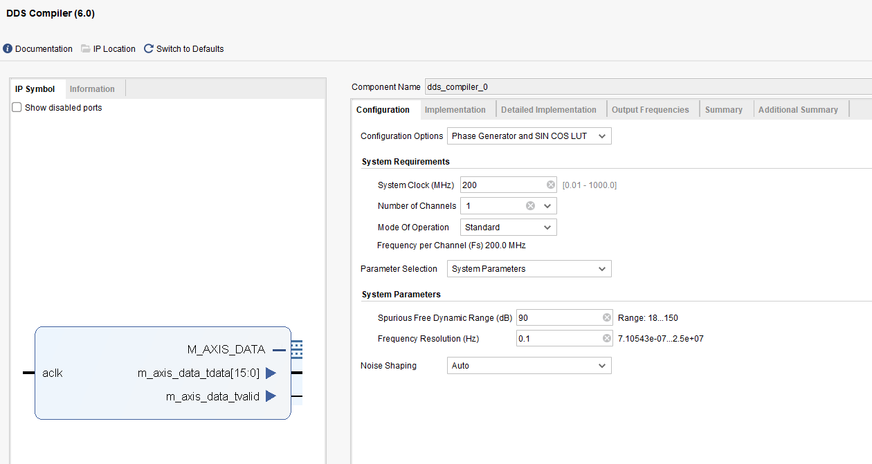
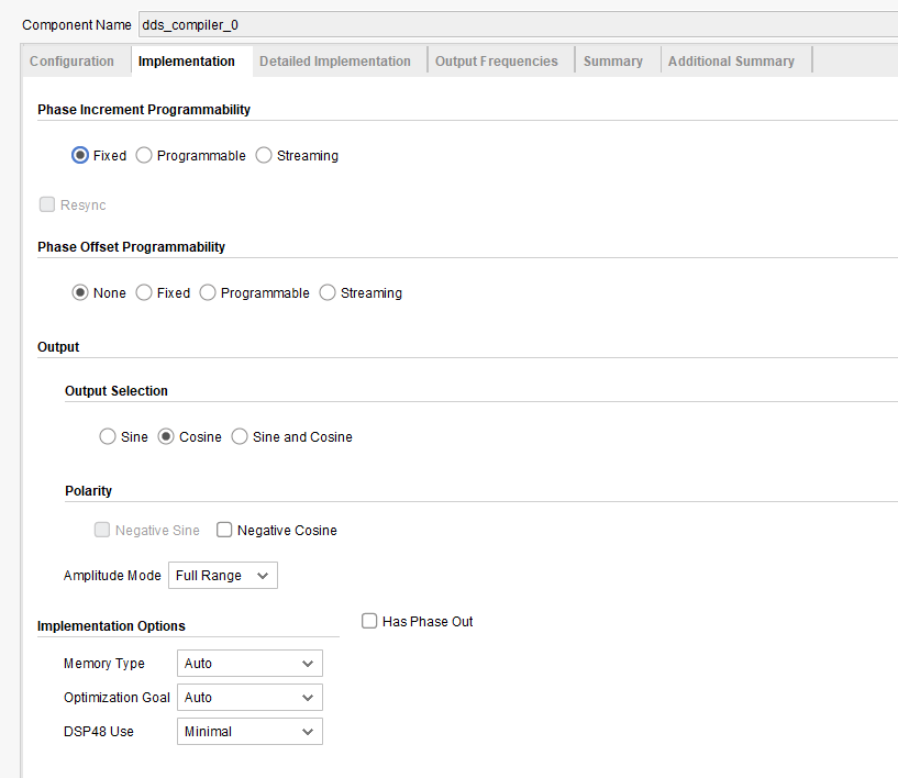
To achieve the desired modulated signal, we need two DDS IP Cores: One that generates the message signal with a 5 KHz frequecy and the other DDS to generate the carrier frequency of 10.7 MHz. I also decided to have a dynamic range of 90 dB and a frequency resolution of 0.1Hz. Below are screenshot showing how each of these DDS IP cores was configured.
Multiplying the Frequency Deviation Δf with cos(2πfmt)
In the FM phase term, the modulating waveform cos(2 π fm t) must be normalized to lie between −1 and +1. This is important because the frequency deviation is proportional to the instantaneous value of the message signal, and exceeding this range would unintentionally increase the modulation index and distort the FM signal.
In my implementation, the message signal is represented in fixed-point format and ranges approximately from −16372 to +16368 (i.e., close to a signed 14-bit full-scale range). I multiply each sample of this message signal by a constant corresponding to the desired frequency deviation of 75 kHz.
This multiplication increases the bit width of the result, so I shift the product right by 14 bits to bring it back to a normalized range. The choice of a 14-bit shift matches the original dynamic range of the message signal, effectively scaling it to approximately −0.99 to +0.99.
This normalization ensures that the modulating signal is properly bounded, so that the applied frequency deviation remains within ±75 kHz, as intended in the FM design.
In this design, a Multiplier IP core is used to multiply the frequency deviation Δf by the normalized message signal generated by the DDS. This operation scales the message signal so that its amplitude produces the desired frequency deviation in the FM modulator.
Since the DDS output and the frequency deviation Δf are represented using fixed-point arithmetic, the result of the multiplication has a wider bit width.
To represent a 75 KHz frequency deviation in a DDS-based FM modulator, the deviation must be converted into a phase increment value that matches the DDS phase accumulator resolution.
For a DDS with a 31-bit phase accumulator and a sampling frequency of 200 MHz, the frequency resolution is:
ΔfLSB = Fs / 231
To achieve a 75 KHz peak frequency deviation, the required DDS phase increment deviation is calculated with the equation below:
ΔPhase Increment = (Δf / Fs) × 2N = 805306. Fs = 200 MHz, and N = 31. N is the phase increment width in bits.
After multiplying the vakue of the frequency deviation with the normalized message signal, the result is added to the value respresenting the Carrier Frequency (10.7 MHz) to the Product of the Message Signal and Frequency Deviation
Using the equation below we computed that the phase increment value for DDS needs to be: 114,890,375 ; for a sampling frequency of 200MHz and phase width of 31 bits.
VHDL Top Level Code
The code below is implemented based on the block diagram below:
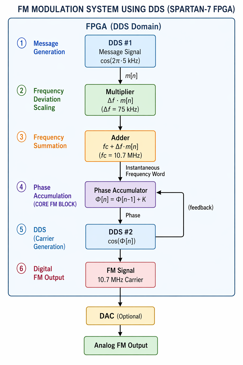
Below is copy of the VHDL top level code. It shows how all the IP core block as connected to each other to generate the final FM modulated signal
This code was implemented on a Xilinix Spartan7 FPGA, and I used a DAC to generate the the recovered baseband signal: 5 KHz that I initially modulated with 10.7 MHz.
library ieee;
use ieee.std_logic_1164.all;
use ieee.numeric_std.all;

entity FM_Modulator_DAC_TopLevel is
  port (
    clk             : in  STD_LOGIC;
    --DDSCLK        : out STD_LOGIC;  --just for TestBench
    reset           : in STD_LOGIC;
    Dac_Out         : out std_logic_vector(11 downto 0);
    --FM_modulation : out std_logic_vector(7 downto 0);  --just for TestBench
    ChipSeclect_n   : out STD_LOGIC;
    WriteEnable     : out STD_LOGIC
  );
end FM_Modulator_DAC_TopLevel;

architecture behavioral of FM_Modulator_DAC_TopLevel is
signal locked_Sig               : std_logic;
signal m_axis_data_tvalid_Sig   : std_logic;
signal Message_Tone             : STD_LOGIC_VECTOR(15 DOWNTO 0);
signal MessageMultiplied        : STD_LOGIC_VECTOR(35 DOWNTO 0);
signal MessageMultipliedShifted : STD_LOGIC_VECTOR(22 DOWNTO 0);
signal DDS1_tvalid_out          : STD_LOGIC;
signal ModulatedSignalOut       : STD_LOGIC_VECTOR(7 DOWNTO 0);
signal Fm_Plus_Carrier          : STD_LOGIC_VECTOR(31 DOWNTO 0);
signal Fm_Plus_Carrier_Pudded   : STD_LOGIC_VECTOR(31 DOWNTO 0);
signal ModulatedSignalOut_DAC_In : STD_LOGIC_VECTOR(11 DOWNTO 0);
signal ChipSeclect_n_sig     : std_logic := '0';
signal DACSample_Sig         : std_logic := '0';
signal WriteEnable_IntSig    : std_logic:= '0';

signal temp           : std_logic_vector( 0 downto 0);
signal Dac_Out_Sig    : std_logic_vector(11 downto 0);
signal DAC_in_pulse   : std_logic:= '0';
signal tmp            : signed(35 downto 0);

signal clk100MHz  :std_logic;
signal clk200MHz  :std_logic;
signal clk10MHz   :std_logic;

-- State machine state
signal state : integer := 0;

signal BasebandSignal    : std_logic_vector(67 downto 0);
signal BasebandSigScaled : std_logic_vector(11 downto 0);
signal counter           : integer range 0 to 19 := 0;
signal ADC_in_sig        : std_logic_vector(7 downto 0);
signal FMsignal_12Bits   : STD_LOGIC_VECTOR(11 DOWNTO 0);
signal DACcounter        : integer range 0 to 499 := 0;

component clk_wiz_0
port
 (
  clk_out1          : out std_logic;
  clk_out2          : out std_logic;
  clk_out3          : out std_logic;
  locked            : out std_logic;
  clk_in1           : in  std_logic
 );
end component;

COMPONENT dds_compiler_0
  PORT (
    aclk               : IN STD_LOGIC;
    m_axis_data_tvalid : OUT STD_LOGIC;
    m_axis_data_tdata  : OUT STD_LOGIC_VECTOR(15 DOWNTO 0)
  );
END COMPONENT;

COMPONENT mult_gen
  PORT (
    CLK : IN STD_LOGIC;
    A   : IN STD_LOGIC_VECTOR(15 DOWNTO 0);
    P   : OUT STD_LOGIC_VECTOR(35 DOWNTO 0)
  );
END COMPONENT;

COMPONENT c_addsub_0
 PORT (
     A  : IN STD_LOGIC_VECTOR(22 DOWNTO 0);
    CLK : IN STD_LOGIC;
    S   : OUT STD_LOGIC_VECTOR(31 DOWNTO 0)
  );
END COMPONENT;

COMPONENT dds_compiler_1
  PORT (
    aclk                : IN STD_LOGIC;
    s_axis_phase_tvalid : IN STD_LOGIC;
    s_axis_phase_tdata  : IN STD_LOGIC_VECTOR(31 DOWNTO 0);
    m_axis_data_tvalid  : OUT STD_LOGIC;
    m_axis_data_tdata   : OUT STD_LOGIC_VECTOR(7 DOWNTO 0)
  );
END COMPONENT;

COMPONENT fm_mod_0
  PORT (
    adc_in : IN STD_LOGIC_VECTOR(7 DOWNTO 0);
    clk    : IN STD_LOGIC;
    fm_demodulated : OUT STD_LOGIC_VECTOR(67 DOWNTO 0)
  );
END COMPONENT;

COMPONENT ila_0
PORT (
	clk     : IN STD_LOGIC;
	probe0 : IN STD_LOGIC_VECTOR(11 DOWNTO 0)
);
END COMPONENT  ;

begin
Clk_Wizard: clk_wiz_0
   port map (
   clk_out1 => clk100MHz,
   clk_out2 => clk200MHz,
   clk_out3 => clk10MHz,
   locked   => locked_Sig,
   clk_in1  => clk
 );
DDS_0 : dds_compiler_0
  PORT MAP (
    aclk => clk200MHz,
    m_axis_data_tvalid => m_axis_data_tvalid_Sig,
    m_axis_data_tdata  => Message_Tone
  );
Multiplier : mult_gen
  PORT MAP (
    CLK => clk200MHz,
    A => Message_Tone,
    P => MessageMultiplied
  );
tmp <= shift_right(signed(MessageMultiplied), 14);
MessageMultipliedShifted <= std_logic_vector(tmp(22 downto 0));

AdderSub : c_addsub_0
  PORT MAP (
    A   => MessageMultipliedShifted,
    CLK => clk200MHz,
    S   => Fm_Plus_Carrier
 );
DDS1 : dds_compiler_1
 PORT MAP (
   aclk => clk200MHz,
   s_axis_phase_tvalid => '1',
   s_axis_phase_tdata =>  Fm_Plus_Carrier,
   m_axis_data_tvalid => DDS1_tvalid_out,
   m_axis_data_tdata => ModulatedSignalOut
);
end behavioral;
Simulation Results
Below are screen shots taken from Vivado simulation showing the FM modulation signal for 5Hz message signal.
The output waveform shows a sinusoidal signal whose frequency varies over time according to the message signal.
- When the message signal is at its positive peak, the FM signal is at maximum frequency (fc + Δf): 10.7 MHz + 75 KHz = 10.775 MHz
- When the message signal is at its zero crossing, the FM signal is at carrier frequency (fc): 10.7 MHz
- When the message signal is at its negative peak, the FM signal is at minimum frequency (fc − Δf): 10.7 MHz − 75 KHz = 10.625 MHz


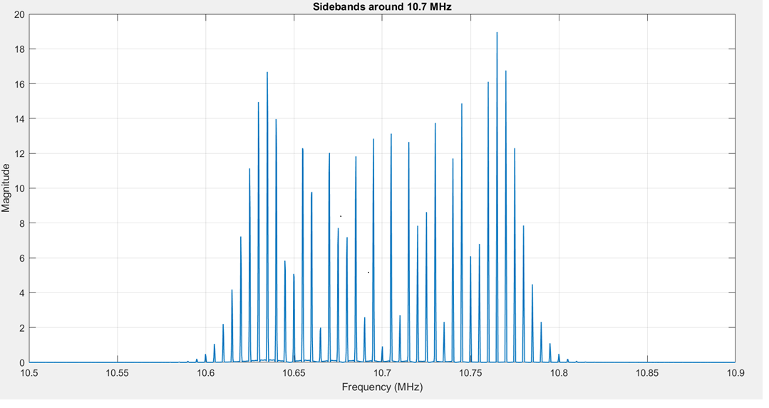
The FFT of the output signal shows: A carrier centered at the desired frequency, and Sidebands spaced according to the message frequency.
The FFT of the FM signal reveals sidebands symmetrically spaced around the carrier fc = 10.7 MHz at fc ± nfm, where n = 1, 2, 3, 4 …
The detected frequency on the plot goes from 10.605 MHz with an increment of 5 KHz.
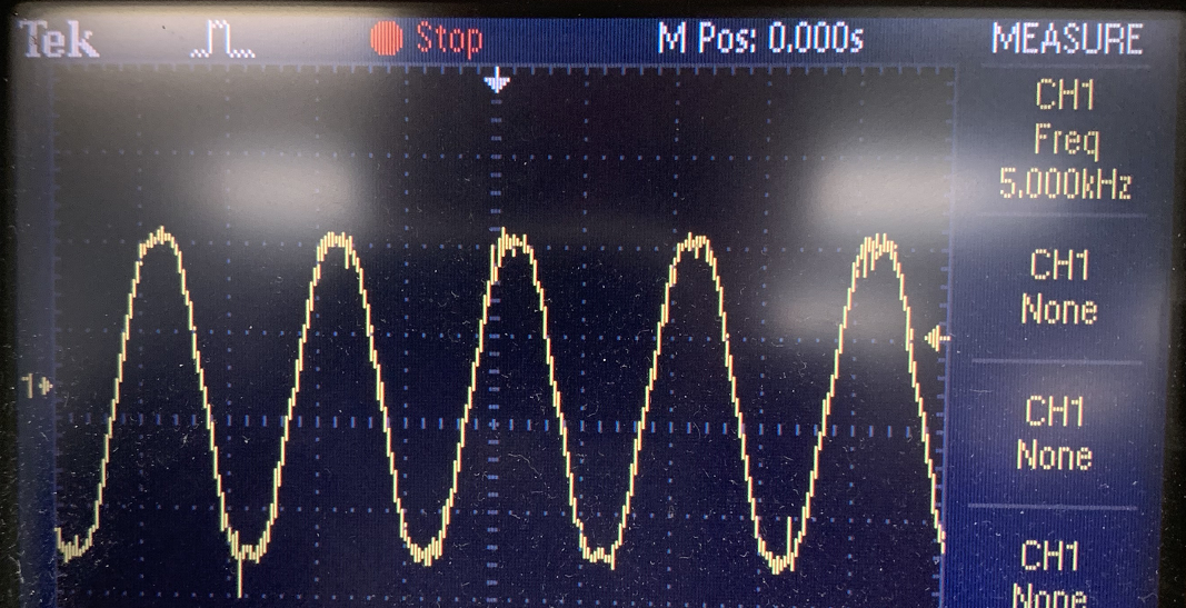
Using an FM demodulated IP core I developed on system generator, I validated the modulated signal and the scope shows the recovered message signal of 5KHz.
Frequency Spectrum
For the given FM modulation with a carrier frequency of 10.7 MHz, a modulating frequency of 5 KHz, and a peak frequency deviation of 75 KHz, the resulting spectrum consists of a series of discrete spectral lines located at
fc ± n fm, where n = 0, 1, 2, …. These lines are spaced by the modulating frequency (5 KHz) and their amplitudes are determined by the modulation index
β = Δf / fm = 75000 through the Bessel functions of the first kind.
Because the modulation index is large (β >> 1), many sidebands carry significant energy, resulting in a wideband FM signal. This shows that the modulation index controls the distribution of energy across the sidebands and directly affects how “wide” the FM signal appears in the frequency domain.
According to Carson’s rule, the approximate total bandwidth occupied by the FM signal is
B ≈ 2(Δf + fm) = 160 KHz. This means most of the spectral energy lies roughly here: 10.7 MHz±80 kHz.
In summary, the frequency deviation determines the number and relative strength of the sidebands, while the spacing between the spectral lines remains fixed by the modulating frequency. This is why, even for large deviations, the sidebands occur at multiples of the modulating frequency around the carrier.
Source Code
For the full VHDL project files, you can visit the GitHub repository:
FM Modulation with DDS 10.7MHz Project
.
Conclusion
A digital FM modulator is implemented successfully on Xilinix FPGA, the results were simulated and validated on real hardware. The modulated signal was recovered in reat time with a digital demodulator.
By leveraging the flexibility of DDS and FPGA-based processing, it is possible to build a fully programmable FM modulator suitable for communication and signal processing applications.
I hope you will find this tutorial helpful, and I would really appreciate any feedback or comments in the comments section and via emails.
Author: Farid M

