
In this post, I will be talking about the design of a digitally controlled DC-DC buck converter, based on peak current mode control theory. All the discussions coming up are based on this TI application note[1]. Also it is assumed that the reader has sufficient knowledge about buck converters design, control theory in general and peak current mode control theory in particular. However, if the reader needs to refresh their mind or get familiar with DC-DC buck converters designs and peak current mode control theory, these links[1] and [2] are very useful for this purpose.
The firmware for this DC-DC buck converter was designed on a TI C2000 DSP MCU: MTS320F2869, and it was tested with this MCU development board, MCU F28069M LaunchPad: https://amzn.to/2SRTyf8, and a digital power buck converter board:BOOSTXL-BUCKCONV.
The design requirement of this project is to generate a +4VDC output voltage that can delivers up to 2A output current. The system is supposed to be stable with a phase margin of at least 45 degrees, and it has to have a crossover frequency equal to 15KHz.
The figure below shows a copy of the schematics for this DC-DC buck converter development board used in the validation of my source code.
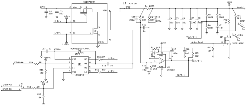 Figure1: DC-DC Buck Converter Schematics[3]
Firmware Implementation
The diagram below shows all the components making up this DC-DC buck converter. The items included in the dashed red lines rectangle are implemented on the MCU, and are going to be discussed in derails in the next paragraphs. Also note that this firmware implementation is totally different in the sample codes discussed in Biricha[1].
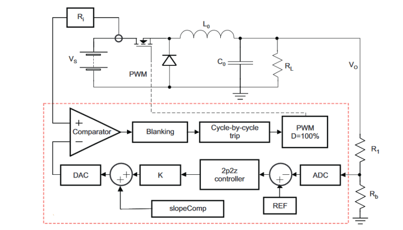 Figure2: Bock Diagram of the entire DC-DC Buck converter[1]
The TMS320F28069 processor has a 32 bits floating point Math processor called: Control Law Accelerator or CLA. It is independent from the CPU and has its own register set, memory bus structure, and processing unit. Since the closed control loop involves intensive computations that need to be completed within very stringent timelines, I decided to use this TI C2000 processor and implement the closed control loop algorithm in the CLA so that so the CPU is released from any overhead. Yet, the CPU still has to service interrupts and perform any non time critical tasks.
Digital Control Loop Algorithm
Pulse Width Modulation: The PWM switching frequency for the MOSFETs: M1 and M2 is selected to be 200KHz. I selected this frequency just to have less current ripples. EPWM4A is used to derive M2 and EPWM4B is used to switch M1. As the two PWM signals need to be complimentary, I used the dead-band sub-module of the EPWM peripheral. EPWM4A have a duty cycle equal to 80%, while EPWM1B has a 40% duty cycle.
EPWM1B is used to trigger the start of ADCINA3 channel conversion. Thus, ADC sampling starts at the falling edge of EPWM1B, and sampling frequency is 200KHz. At the end of ADC conversion a CLA task1 is called to process the sampled data in the control loop.
Output Voltage Feedback: Vout_FB is generated using the voltage divider circuit that consists of R2, R4, and R5. The divider ratio is 0.49, and before this analog input is fed to the ADC channel ADCINA3, it goes through an RC filter made up with R4 and C3. It turned out that the cutoff frequency of this filter is: 48.22KHz. This filter is needed so that high frequencies such as EPWM switching frequencies, which could introduce disturbances on the measured analog signals IL_FB and Vout_FB, are filtered out. Later, Vout_FB is compared to a voltage reference Vref, and the difference between the two values is the error that is the input to the closed loop controller.
Current Feedback: The current sense IL_FB is measured with the help of a sense resistor R1 and a differential operational amplifier. The current sense gain=(1200/82)*(0.03)=0.43. IL_FB is fed to the non inverting input pin of an internal analog comparator: COMP2. The inverting pin of the comparator is connected to the output of a DAC whose output is controlled by the output of the closed loop controller (see figure2). The output of the comparator COMP2OUT is used to turn off EPWM4A whenever IL_FB voltage goes higher than than DAC output.
Slope compensation: In his paper: “A More Accurate Current-Mode Control Model”, Ridley recommended the use of a slope compensation ramp when duty cycle D is 36% or above[6]. As shown in Figure2, the ramp slope compensation needs to be added so that sub-harmonics oscillations does not occur. These oscillations are a result of the current feedback loop. The formula to calculate the Vpp of the slope compensation is:
Vpp=((0.18-D)*Ri*Ts*Vin)/L0=1.88V where D=Vin/Vout=4/9=0.44; Ri=0.43;Vin=9V,Ts=5us;L0=4.8uH.
DigitalRampHeight=Vpp*(1023/3.3)*64=21593. This value is decremented at every clock cycle till it gets to zero at the end of each PWM period. The calculation of the decrement value is as follow:
For every PWM period there is: 5000ns/11.11ns=450 steps; clock frequency is 90MHz and PWM frequency is 200KHz. Thus, the decrement value, DigitalRampHeight/steps=48. This is the value used in slopeval defined in: BuckHardware.h file.
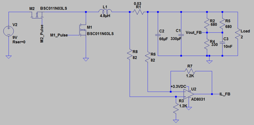 Figure3: Synchronous DC-DC Buck converter
All needed C code files related to the next discussions can be accessed on my GitHub repository at:Github. If anyone needs the entire project, feel free to send me a request by email and I sill send it to you.
I created two CLA tasks: task1 and task4. Task1 is used to process the digital control loop and it is triggered by ADC channel A3 EOC event. computations in this task needs to be completed before the next rising edge of EPWM4A. Task 4 is used to take care of the CLA variables initialization at the start up.
void main(void)
{

// Step 1: Setup the system clock Disable the watchdog timer, initialize the system clock,PLL and configure the peripheral clock.
InitSysCtrl();

// Copy time critical code and Flash setup code to RAM The RamfuncsLoadStart, RamfuncsLoadEnd, and RamfuncsRunStart symbols are created by the linker. Refer to the linker files.
MemCopy(&RamfuncsLoadStart, &RamfuncsLoadEnd, &RamfuncsRunStart);

// Call Flash Initialization to setup flash waitstates This function must reside in RAM
InitFlash(); // Call the flash wrapper init function

//Initialize PIE control Intialize PIE control, disable all interrupts and then copy over the PIE Vector table from BootROM to RAM
DINT; //Disable CPU Interrupts
InitPieCtrl();
IER = 0x00000000;
IFR = 0x00000000;
InitPieVectTable();

// Assign user defined ISR to the PIE vector table
EALLOW;
PieVectTable.CLA1_INT1 = &cla1_task1_isr;
PieVectTable.CLA1_INT4 = &cla1_task4_isr;
EDIS;

// Enable INT11.1 INT 11.2. 11.3 in the PIE (CLA Task1,2,3,4)
PieCtrlRegs.PIEIER11.bit.INTx1 = 1;
PieCtrlRegs.PIEIER11.bit.INTx4 = 1;

/* Enable ADCINT1 in PIE */
PieCtrlRegs.PIEIER1.bit.INTx1 = 1; /* Enable INT 1.1 in the PIE */

//Enable CLA interrupts
IER |= M_INT11;
IER |= M_INT2;

EINT;/* Enable Global interrupt INTM */
ERTM;/* Enable Global realtime interrupt DBGM */

init_cla();

//Configure GPIOs
Gpio_select();

//Configure ADCs
ADCs_Config();

//Configure PWM
PWMs_Config();

//Configure Comparators
Comparator_Config();

GpioDataRegs.GPASET.bit.GPIO10=1; //activate load for buckdevboard

while(1)
{
}

}
The control loop is implemented in three different ways just to explore how each control method works and find out if there is any differences between these algorithms in terms of response time, and stead state errors. I initially implemented the control loop using a Proportional Integrator Differentiator controller using the difference equation below[5].
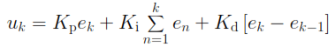 Equation1
KP_Coeff=KP;
KI_Coeff=KI*T_Sample/2;
KD_Coeff=KD/T_Sample; //T_sample=1/200KHz=0.000005.
At the second time, I implemented the PID using Tastin Bilinear Transformation according to the equation below is used:
u[k]=u[k-1]+a*e[k]+b*e[k-1]+c*e[k-2]
Equation2
KP_Coeff=KP;
KI_Coeff=KI*T_Sample/2;
KD_Coeff=KD/T_Sample; //T_sample=1/200KHz=0.000005.

a=KP_Coeff+KI_Coeff+KD_Coeff;
b=KI_Coeff-KP_Coeff-2*KD_Coeff.
c=KD_Coeff.
At the last, I used a two poles two zeros, 2P2Z controller. The equation for this controller is:
u[k]=a1*u[k-1]+a2*e[k-2]+b0*e[k]+b1*e[k-1]+b2*e[k-2]
Equation3
the coefficient a1, a2, b0, b1 and b2 are calculated based on the equations given by Biricha in his notes[1] page6. Biricha also has a design tool that compute these coefficients at this link: https://www.biricha.com/wds.html
PID implementation with Ziegler-Nichols Method:
Task4: it only initializes Voltage reference, and PID coefficients. It runs only one time and it is software triggered, called from main function. Voltage reference and PID coefficients are defined in Compensator_CLA.h. Later, I will explain how the PID coefficients are selected.
Also I needed to compute PID limits: PIDOut_MAX and PIDOut_MIN. PIDOut_MIN is set to zero, while PID_MAX is computed as follow:
The current gain in the circuit of my development board is equal to:R1*(R7/R6)=0.43, see Figure3. Since the DAC can generate a maximum analog voltage equal to +3.3VDC then the maximum current sense we can use with the internal comparator is: 3.3/0.43=7.67A.
I selected a value for PID max to be equal to 2500, and note here that my DAC values have to be scaled by 0.25(DAC resolution/ADC resolution.) This means analog value correspond to 2500 is: 2500*(0.25/1023)*3.3=2.016V. This value corresponds to 4.65A. PIDOut_MAX and PIDOut_MIN values are defined in Compensator_CLA.h.
__interrupt void Cla1Task4 (void)
{
 BuckControl_Ref=0;

 PID2.Delta=0;
 PID2.PIDOuput=0;
 PID2.PIDOuput_K1=0;
 PID2.Error_K0=0;
 PID2.Error_K1=0;
 PID2.Error_K2=0;
 PID2.pidmax=PIDOut_MAX;
 PID2.pidmin=0;

 KP_Coeff=KP;
 KI_Coeff=KI*T_Sample/2;
 KD_Coeff=KD/T_Sample;
}
Task1: computes PID output and also it implements a soft start: gradual turning on of the power supply so that components are not stressed due to inrush currents or voltage surges. Task1 is triggered every 5us, each time it is triggered BuckControl_Ref is incremented by VoutSlewRate, which is equal to 12 in this example, till it reaches the voltage reference value BUCK_ADCREF. This voltage reference is defined in Compensator_CLA.h. It takes 1.013ms ( for Vref to be equal to BUCK_ADCREF value.
Voltage reference BUCK_ADCREF is computed as follow: Vout=+4VDC; ADC is 12 bits meaning that the resolultion is: 1/4095; Voltage divider ratio is:R4/(R4+(R2//R5))=0.49. Thus, Vref=1/ADCresolution*Vout*0.49/3.3=2432. It takes 1.013ms ( 2432/12)*5us) for Vref to be equal to BUCK_ADCREF value. The user can change this soft start time if needed by varying VoutSlewRate.
__interrupt void Cla1Task1 (void)
{
__mdebugstop();

if(BuckControl_Ref < BUCK_ADCREF)
{
BuckControl_Ref+= VoutSlewRate;
}
else
{
BuckControl_Ref=BUCK_ADCREF;
}

PID2.CurrInput=(float) AdcResult.ADCRESULT0;
PID2.Error_K0= BuckControl_Ref-PID2.CurrInput;

//proportional term
PID2.Kp_Term= KP_Coeff*PID2.Error_K0;

//Integrator term
PID2.Integeral_Term= PID2.Integeral_Term+ KI_Coeff*PID2.Error_K0;
PID2.Integeral_Term=PID2.Integeral_Term+PID2.Delta;

//Derivative term
PID2.D_Input= PID2.CurrInput-PID2.PastInput;

// Compute PID Output
PID2.PIDOuput= PID2.Kp_Term+ PID2.Integeral_Term- KD_Coeff*PID2.D_Input;
if(PID2.PIDOuput > PIDOut_MAX)
{
PID2.Delta=PIDOut_MAX-(PID2.PIDOuput); //added for anti windup
PID2.Delta=PID2.Delta*1;
PID2.PIDOuput = PIDOut_MAX;
}
else if(PID2.PIDOuput < PIDOut_MIN)
{
PID2.Delta=PIDOut_MIN-(PID2.PIDOuput); //added for anti windup
PID2.Delta=PID2.Delta*1;
PID2.PIDOuput = PIDOut_MIN;
}
else
{
PID2.Delta=0;
}
PID2.PastInput=PID2.CurrInput;
//for debugging
temp2=PID2.Error_K0;

MEALLOW;
Comp2Regs.RAMPMAXREF_SHDW = PID2.PIDOuput*16; //Cmpns2.Out*2^10*2^16; Cmpns3 is an analog value scaled by (1/3.3)*2e12
//Comp2Regs.DACVAL.all = PID2.PIDOuput*0.25; // 2e10/2e12
MEDIS;
PID Coefficients Calculation and Tuning:
I used Ziegler-Nichols turning method[4] to set KP, KI and KD. First, I set KI and KD to zero and at the same time, I set KP to 5. These values can be modified from Compensator_CLA.h header file. I kept increasing KP till I started to see oscillations on the output voltage, and this happens when KP is equals to 12, see Figure4. This value is denoted as Kcr. Then I measured the period of osculations, Pcr, and I found that it is equal 40 us. Ziegler-Nichols theory says that: KP=0.6 Kcr, KD=1/0.5*Pcr, and KD=0.125Pcr. The coefficients turned out to be: KP=6.5; KI=50000; KD=0.00005. Figure5 shows that settling time here is around 1ms, and no overshoot.
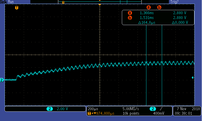 Figure4: Voltage output response when KP=12, KI=0, and KD=0
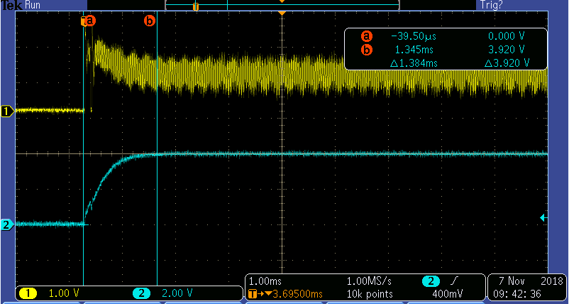 Figure5: Voltage output response after tuning when KP=6.2, KI=50000, and KD=0.000005
The Plot below shows the steady state error: PID2.Error_K0 for the voltage output. If you wonder how this plot is obtained, I can share with you how: Inside __interrupt void Cla1Task1 (void) function, PID2.Error_K0 value is copied into a CLA variable temp2. In main.c file, there is a __interrupt void cla1_task1_isr(void) function which is used to clear the CLA task1 interrupt, and inside this ISR service routine, I read the value of the variable temp2 into an array of 2000 elements, PID2outArray. Since this interrupt is triggered every 5us, it means I was sampling data for 2000*5us=10000us or 10ms. If you notice inside cla1_task1_isr() you will see that I am toggling GPIO 22.
__interrupt void
cla1_task1_isr(void)
{
  static int b=0;

  AdcRegs.ADCINTFLGCLR.bit.ADCINT1 = 1;
  PieCtrlRegs.PIEACK.bit.ACK11 = 1;

  GpioDataRegs.GPATOGGLE.bit.GPIO22=1;

  if(b<2000)
  {
     PID2outArray[b]=temp2;
     b++;
   }

}
To plot the data obtained, I went to debug mode in the code composer, then go to view and from there select Memory Browse. Inside memory browse window type: &PID2outArray, select type of data as 32 bits floating point. Then, go to Tools and select save data. Data will be saved into a file that can be exported to an excel file from which plots can be obtained.
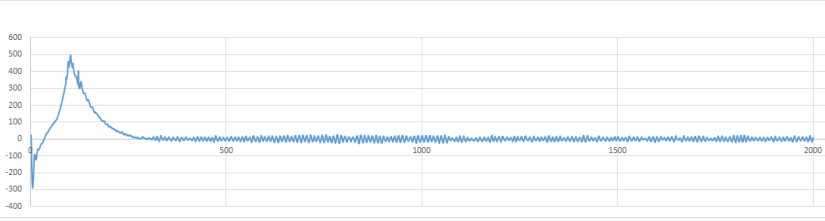 figure6: PID2.Error_K0 for the voltage output.
If you notice inside cla1_task1_isr() you will see that I am toggling GPIO 22. This is used to estimate how much time it takes for the control loop math to be completed. As seen in the plot below this computation time takes about 2us, and it has to be completed before the rising edge of EPWM4A( proble6), which switches the MOSFET M2. Note here that EPWM4B(proble7) switches MOSFET M1. Also I want to mention that the computation process starts at the falling edge of EPWM1B (Probe1). Probe0 in the plot is for EPWM1A.
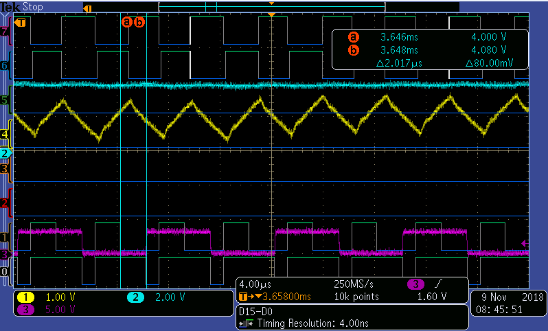 figure6: Buck signals: Blue: Vout; Yellow: Inductor Current; Purple: GPIO22.
PID implementation with Bilinear Transform:
The values of coefficients: KP_Ceoff, KI_Ceoff, and KD_Ceoff that we found in using Ziegler-Nichols method are used in this implementation to compute constants a, b and C of Equation2. The controller limits OutMax and OutMin are the same as PIDOut_MAX and PIDOut_MIN that I computed earlier.
Cmpns2_Coef.b0=KP_Coeff+KI_Coeff+KD_Coeff;
Cmpns2_Coef.b1=KI_Coeff-KP_Coeff-2*KD_Coeff;
Cmpns2_Coef.b2=KD_Coeff;
__interrupt void Cla1Task4 (void)
{

BuckControl_Ref=0;

KP_Coeff=KP;
KI_Coeff=KI*T_Sample/2;
KD_Coeff=KD/T_Sample;

Cmpns2_Coef.b0=KP_Coeff+KI_Coeff+KD_Coeff;
Cmpns2_Coef.b1=KI_Coeff-KP_Coeff-2*KD_Coeff;
Cmpns2_Coef.b2=KD_Coeff;
Cmpns2_Coef.a1=1;
Cmpns2_Coef.a2=0;
Cmpns2_Coef.OutMax=Max; // Parameter: Maximum output
Cmpns2_Coef.OutMin=Min; // Parameter: Minimum output

Cmpns2.Ref=BuckControl_Ref; // Input: Reference input
Cmpns2.Fdb=0; // Input: Feedback input
Cmpns2.Errn=0; // Variable: Error
Cmpns2.Errn1=0; // Parameter: Proportional gain
Cmpns2.Errn2=0; // Variable: Proportional output
Cmpns2.Out=0; // Variable: Integral output
Cmpns2.Out1=0; // Variable: Derivative output
Cmpns2.Out2=0; // Variable: Derivative output
Cmpns2.OutPreSat=0; // Variable: Pre-saturated output
}
Digital closed control loop implementation using Tustin Method. A soft start is also used as in the previous implementation.
__interrupt void Cla1Task1 (void)
{
__mdebugstop();

//Soft start
if(BuckControl_Ref < BUCK_ADCREF)
{
BuckControl_Ref+= VoutSlewRate;
}
else
{
BuckControl_Ref=BUCK_ADCREF;
}

Cmpns2.Ref=BuckControl_Ref;
Cmpns2.Fdb=(float) AdcResult.ADCRESULT0; //Multiply by 1/(2^12) to convert it to per unit float;

/* Compute the error */
Cmpns2.Errn=Cmpns2.Ref-Cmpns2.Fdb;
// PreSat = e(n-2)*B2 + e(n-1)*B1 + e(n)*B0 + u(n-2)*A2 + u(n-1)*A1
Cmpns2.OutPreSat = Cmpns2_Coef.b2*Cmpns2.Errn2 +Cmpns2_Coef.b1*Cmpns2.Errn1 + Cmpns2_Coef.b0*Cmpns2.Errn + Cmpns2_Coef.a2*Cmpns2.Out2 + Cmpns2_Coef.a1*Cmpns2.Out1;
/* store history of error*/
Cmpns2.Errn2 = Cmpns2.Errn1;
Cmpns2.Errn1 = Cmpns2.Errn;
Cmpns2.Out=Cmpns2.OutPreSat;
/* Saturate the output, use intrinsic for the CLA compiler */
Cmpns2.Out=__mminf32(Cmpns2.Out,Cmpns2_Coef.OutMax);
Cmpns2.Out=__mmaxf32(Cmpns2.Out,Cmpns2_Coef.OutMin);
/* store the history of outputs */
Cmpns2.Out2 = Cmpns2.Out1;
Cmpns2.Out1 = Cmpns2.Out;

MEALLOW;
//Comp2Regs.DACVAL.all = Cmpns2.Out*1023; //Multiply by 2^6, because this is Q10
Comp2Regs.RAMPMAXREF_SHDW=Cmpns2.Out*16; //Cmpns1.Out*2^10*2^6;
MEDIS;

temp2=Cmpns2.Errn; //used for debugging and plotting steady state error
}
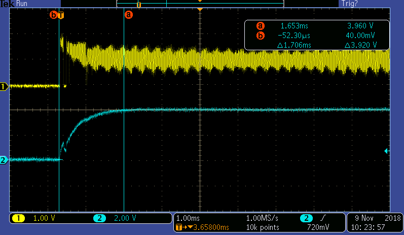 Figure7: Output Voltage and inductor current using Bilinear Transform PID
The plot below shows the steady state error for the voltage output. I could tell by comparing the two plots: Figure6 and Figure8 that Bilinear Transform produces better results in terms of stead state error. However, the response time and overshoot are the same.
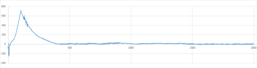
figure8: PID2.Error_K0 plot for the voltage output using Tustin method PID
2P2Z Controller Implementation
This implementation uses Equation3 discussed previously and I used the equations defined in[1] page 6 to calculate constants: a1,a2,b0,b1,and b2 needed for this equation. The calculated constants are defined in Compensator_CLA.h file.
#define a1_Coef 0.8285976581
#define a2_Coef 0.1714023419
#define b0_Coef 4.1703226660
#define b1_Coef -5.9120992707
#define b2_Coef 1.9495912223
Task4 is used to initialize variables used in the closed control loop. The controller limits OutMax and OutMin are simlilar to the limits used in the previous implementations: OutMax=2500; and OutMin=0.
__interrupt void Cla1Task4 (void)
{
BuckControl_Ref=0;
temp2=0;

Cmpns2_Coef.b0=b0_Coef;
Cmpns2_Coef.b1=b1_Coef;
Cmpns2_Coef.b2=b2_Coef;
Cmpns2_Coef.a1=a1_Coef;
Cmpns2_Coef.a2=a2_Coef;
Cmpns2_Coef.OutMax=Max; // Parameter: Maximum output
Cmpns2_Coef.OutMin=Min; // Parameter: Minimum output

Cmpns2.Ref=BuckControl_Ref; // Input: Reference input
Cmpns2.Fdb=0; // Input: Feedback input
Cmpns2.Errn=0; // Variable: Error
Cmpns2.Errn1=0; // Parameter: Proportional gain
Cmpns2.Errn2=0; // Variable: Proportional output
Cmpns2.Out=0; // Variable: Integral output
Cmpns2.Out1=0; // Variable: Derivative output
Cmpns2.Out2=0; // Variable: Derivative output
Cmpns2.OutPreSat=0; // Variable: Pre-saturated output
}
In terms of the code used in Cla1Task1, the implementation of the control loop is similar to the implementation used with Bilinear Transform. The reason is that PID is nothing but a special case of 2P2Z controller, where the constants of the 2p2z: a1=1, and a2=0.
__interrupt void Cla1Task1 (void)
{

//Soft start
if(BuckControl_Ref < BUCK_ADCREF)
{
BuckControl_Ref+= VoutSlewRate;
}
else
{
BuckControl_Ref=BUCK_ADCREF;
}

Cmpns2.Ref=BuckControl_Ref;
Cmpns2.Fdb=(float) AdcResult.ADCRESULT0; //Multiply by 1/(2^12) to convert it to per unit float;

/* Compute the error */
Cmpns2.Errn=Cmpns2.Ref-Cmpns2.Fdb;
// PreSat = e(n-2)*B2 + e(n-1)*B1 + e(n)*B0 + u(n-2)*A2 + u(n-1)*A1
Cmpns2.OutPreSat = Cmpns2_Coef.b2*Cmpns2.Errn2 +Cmpns2_Coef.b1*Cmpns2.Errn1 + Cmpns2_Coef.b0*Cmpns2.Errn + Cmpns2_Coef.a2*Cmpns2.Out2 + Cmpns2_Coef.a1*Cmpns2.Out1;
/* store history of error*/
Cmpns2.Errn2 = Cmpns2.Errn1;
Cmpns2.Errn1 = Cmpns2.Errn;
Cmpns2.Out=Cmpns2.OutPreSat;
/* Saturate the output, use intrinsic for the CLA compiler */
Cmpns2.Out=__mminf32(Cmpns2.Out,Cmpns2_Coef.OutMax);
Cmpns2.Out=__mmaxf32(Cmpns2.Out,Cmpns2_Coef.OutMin);
/* store the history of outputs */
Cmpns2.Out2 = Cmpns2.Out1;
Cmpns2.Out1 = Cmpns2.Out;

MEALLOW;
//Comp2Regs.DACVAL.all = Cmpns2.Out*1023; //Multiply by 2^6, because this is Q10
Comp2Regs.RAMPMAXREF_SHDW=Cmpns2.Out*16; //Cmpns1.Out*2^10*2^6;
MEDIS;

temp2=Cmpns2.Errn; //used for debugging

}
Voltage output and inductor current when control loop is implemented with a 2p2z controller. Apparently, I dont see any difference between all implementations in terms of setting time, and overshoot.
 Figure9: Output Voltage and inductor current using 2p2Z Controller
Even though we have not seen much difference in terms of response time and overshoot between the three different controller implementations, I certainly can say that the 2P2Z controller yielded good results in terms of the steady state error, it become zero eventually after 500 samples: 500*5us=2500us=2.5ms.
 Figure10: PID2.Error_K0 plot for the voltage output using 2P2Z Controller
Conclusion
This DC-DC buck converter demo project I discussed here can be extended to other higher power requirements provided the right hardware designs are in place. The closed loop controller can also be used to for other DC-DC topological such as Boost and Buck-Boost converters if peak current mode control is used as a control scheme. I personally used this digital closed loop controller and MCU for 10KW applications for both Buck and Boost converters. Next time, I will be talking about the implementation of a three phase interleaved DC-DC buck converter. Stay tuned! Feel free to send me comments/questions whenever you need to.
References
- http://www.ti.com/lit/an/sprabe7a/sprabe7a.pdf
- http://www.ti.com/lit/an/slva477b/slva477b.pdf
- http://www.ti.com/lit/ug/tidu986/tidu986.pdf
- http://techteach.no/publications/articles/zn_closed_loop_method/zn_closed_loop_method.pdf
- http://users.abo.fi/htoivone/courses/isy/DiscreteTimeSystems.pdf
- http://www.ridleyengineering.com/images/current_mode_book/CurrentModeControl.pdf
