
Author: Farid M, https://embeddeddesign.org/
In this tutorial, I will show you how to add a custom AXI IP block and transfer data from the Processing System to the Programming Logic on AXI4 Data Bus in Xilinix Vivado tool development, using Zedboard development board.
I will create a simple adder in VHDL that will add two numbers. The user will enter two values to sum on the PS, as inputs to the PL, and the PL will sum up these values. The will display the sum on Tera Term. All the data transfer takes place on AXI4 peripheral.
More information about AXI4 protocol can be found at this link: AXI Reference Guide
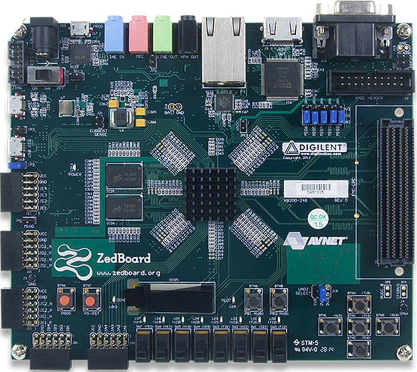
Figure1. Zedboard Development board
Create a new Vivado Project
In this demo, I am using Vivado 16.4. Next, I will show how to start creating the Adder custom IP.
Open Vivado from the start menu and create a new project, and save it in your working directory. I named this project AXI4_Demo. Then hit next and select RTL Project, next select Zedboard Zynq as your target hardware. Then, the project window will open up after you hit finish.
Create Block Design
Under IP Integrator, select Create Block design, and name it. Click Add IP and search for ZYNQ7 Processing System, once you make the selection the block diagram will show up as in the figure below: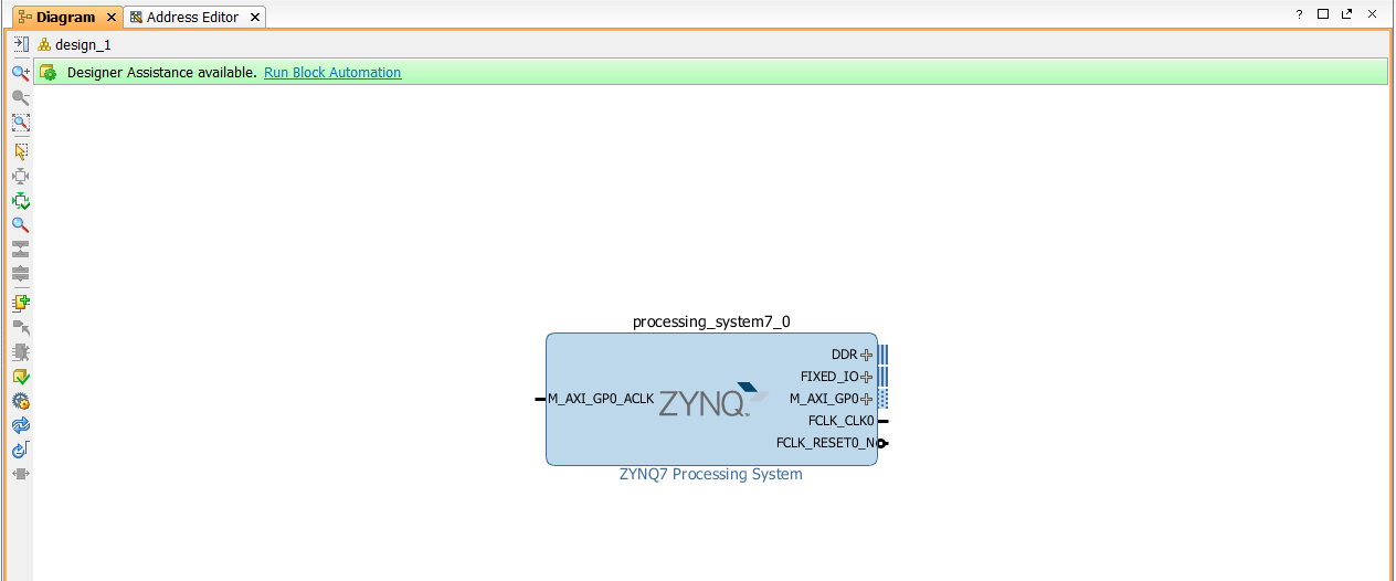
Figure2. ZYNQ7 Processing System
Create Adder VHDL Code
Next, we need to create the VHDL logic for the adder we need to interface with the PS via AXI4 peripheral.
Create a sub-folder in the Vivado project folder, and name it VHDL. Then copy this code shown below into a text editor and save as it as a Adder.vhd under the VHDL sub-folder you created.
------------------------------------------------------------
-- Engineer: F.Mabrouk
------------------------------------------------------------
library ieee;
use ieee.std_logic_1164.all;
use ieee.numeric_std.all;

entity Adder_Unsigned is
port (
FirstValue : in std_logic_vector(30 downto 0);
SecondValue : in std_logic_vector(30 downto 0);
Sum : out std_logic_vector(31 downto 0)
);
end Adder_Unsigned;

architecture rtl of Adder_Unsigned is

begin

Sum <= std_logic_vector(resize(unsigned(FirstValue),32)+resize(unsigned(SecondValue),32));

end rtl;
Create Adder IP
On the Tools menu, select Create and Package New IP, hit next and select Create a New AXI4 Peripheral, hit next and name the IP. I named it: AdderDemoIP, hit next and keep everything as shown below:
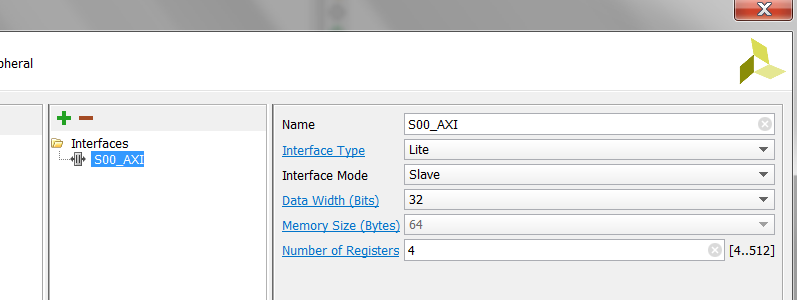 Figure3. AXI4 configuration
Here we have selected 4 registers of 32 bit data width. Then, hit next and select Edit IP, and click Finish. A new window will open up, where will will edit the newly created IP .
Now we need to add the VHDL file we wrote to the newly created IP. From the project menu select Add Sources, and hit next and then select Add Files. Then add the Adder.vhd file you saved. Then go to AdderDemoIP_v1_0_S00_AXI_inst file and do the following changes:
Add this piece of code just above begin (line120):
signal SUMSig : std_logic_vector(31 downto 0);
component Adder_Unsigned
port (
FirstValue : in std_logic_VECTOR(30 downto 0);
SecondValue : in std_logic_VECTOR(30 downto 0);
Sum : out std_logic_VECTOR(31 downto 0));
end component;
At line 390 add this:
 -- Add user logic here
Adder_0 : Adder_Unsigned
port map (
FirstValue=> slv_reg0(30 downto 0),
SecondValue => slv_reg1(30 downto 0),
Sum=> SumSig);
-- User logic ends
Al line 363 change that line of code into this:
reg_data_out <= SumSig;
At line 352 do the following change:
process(slv_reg0,slv_reg1, SumSig, slv_reg3, axi_araddr, S_AXI_ARESETN, slv_reg_rden)
When you are done, hit save and you will see that the files hierarchy changed, and it looks as below:
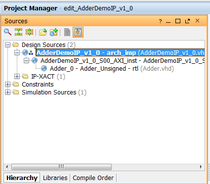
Figure4. Adder IP files Hierarchy
Now, click on Package IP and hit File Groups then click on Merge Changes from File Groups. Then click on Review and Package and click on Re-Package IP, then hit close so that the newly created window for IP configuration is closed.
Now, on the main project window, where the PS diagram is shown, click and Add IP and look for: AdderDemoIP. Once you find it, double click on it so that it is added to the project. Click on Run Block Automation and then click on Run Connection Automation.Then click on Regenerate Layout. When your done click on Validate Design to make sure there is no errors. Then save it. Your system block diagrams will look as below:
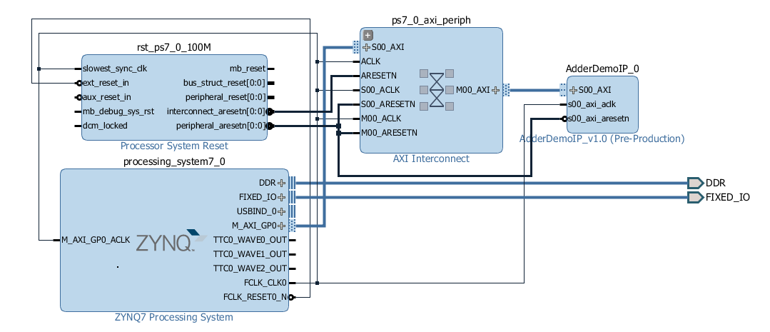
Figure5. System block diagram
Under Block Designs, right hand click on design_1 and select Create HDL Wrapper. Then again right hand click on design_1 and select Generate Output Products, then select Out of Context per IP, and hit Generate. When this process is done, hit Ok. Then from the Flow Navigator on the main menu on the left select Generate Bit Stream.
SDK Project
Once the bit stream is generated, go File on the left top corner and click on Export, then Export Hardware, and select Include Bitstream, then hit Ok. Then, right hand click on File again and hit Launch SDK. The SDK project will open up automatically and it should look as below:
 Figure6. SDK Project Window
Click on File on top left corner and select New and then select Application Project. Name the project: Adder, then click next and select Hello World and hit Finish.
Now if you look under Adder in the Project Explorer to the left you will see a folder named src. If you click on scrc you will a file named: helloworld.c. Right hand click on this file and select rename and name it: Adder.c.
Now open the file Adder.c, and delete its content, and paste the following source code instead, and then build the project.
#include "platform.h"
#include "xbasic_types.h"
#include "xparameters.h"
#include "sleep.h"
#include "xtime_l.h"

Xuint32 *baseaddr_p =XPAR_ADDERDEMOIP_0_S00_AXI_BASEADDR;

int main()
{
init_platform();

xil_printf("AXI4 Adder IP Demo\n\r");

*(baseaddr_p+0) = 77;
*(baseaddr_p+1) = 23;
while(1)
{
	// Register 0
	xil_printf("First Value: %d \n\r", *(baseaddr_p+0));

	// Register 1
	xil_printf("Second Value: %d \n\r", *(baseaddr_p+1));

	//Register 2
	xil_printf("Sum of first and second values is: %d \n\r", *(baseaddr_p+2));

	xil_printf("End of test\n\n\r");

	sleep(1);

	*(baseaddr_p+0)=*(baseaddr_p+0)+1;
	*(baseaddr_p+1)=*(baseaddr_p+1)+1;
}

return 0;
}
Zedboard Connection to Serial Ports
Connect the Zedboard as in the image blow: Verify that the two serial ports ( top left corner of the picture ) are connected to your PC: one serial port is used for programming the FPGA and other serial port is used for communication with Tera term. Also make sure the the power switch is ON. A green LED will be on when the board is powered up.
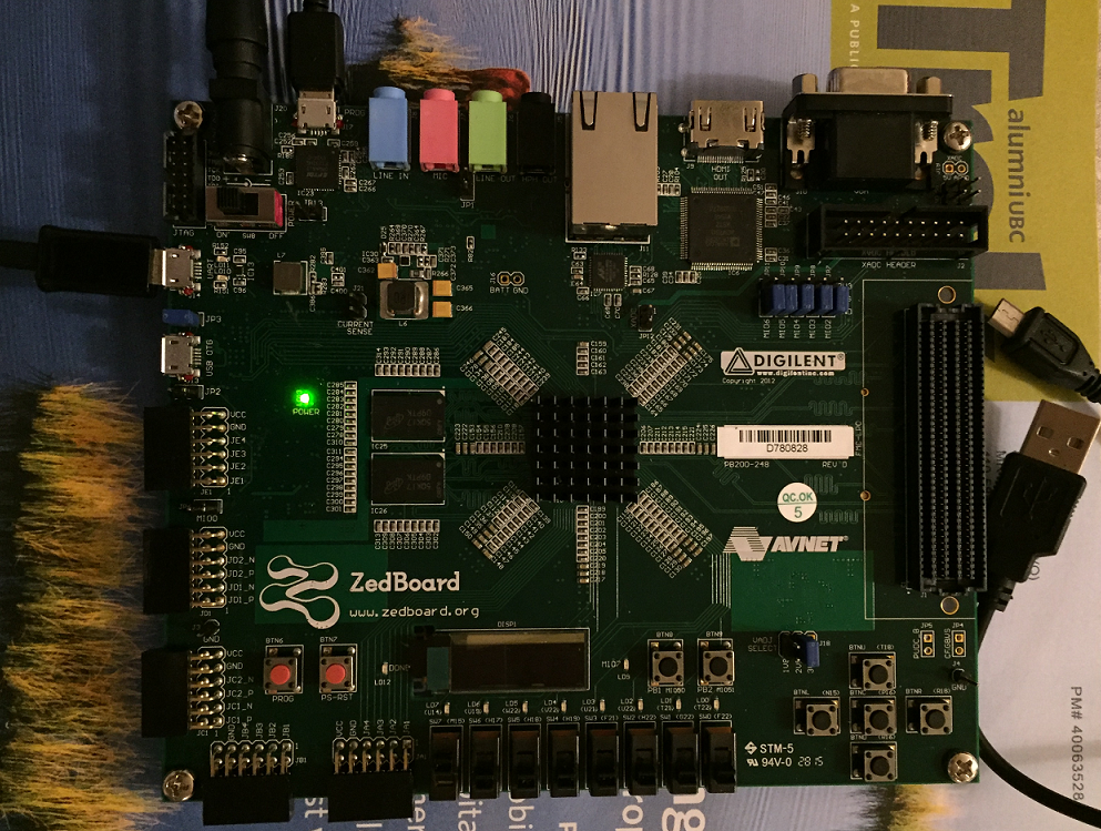 Figure7. Zedboard Serial Port Communication Connections
Serial Port Configuration
Open Tera Term and select connection to USB serial port, then set the correct baud rate by going to Setup and then selecting Serial Port. Set the baud rate to 115200 bps. Click again on Setup and select Terminal, then check Local Echo and change New-line receive and Transmit to: LF and then hit Ok. Below are images of the serial port and terminal setup:
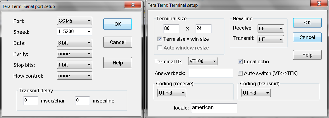 Figure8. Tera Term Configuration
Programming the FPGA
After you have built the project with no errors, click on Xilinx Tools on top menu and select Program FPGA. When it is programmed a blue LED will turns ON. Then, click on Run As ( by right hand clicking on project name) and select Launch on Hardware. Then you will see the following display on Tera Term. This display concludes this tutorial and it proves that sum of any two values is correct, and that the AXI4 data transfer is working as it should
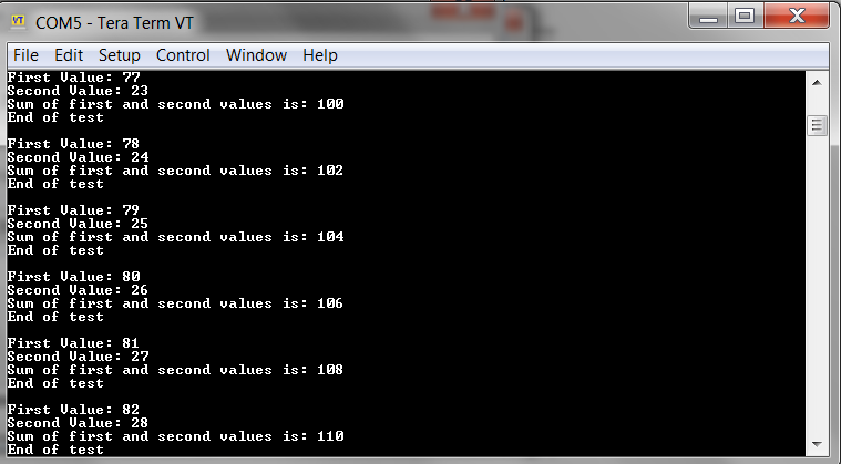
Figure9: Adder Custom IP Test Results
Conclusion
A custom adder IP has been added where AXI4 communication interface between PS and PL has been implemented. In the next tutorial, I will show you how to use AXI4 to control GPIOs/LEDs on the Zedboard development kit.
Author: Farid M, https://embeddeddesign.org/
If you find any of the projects posted here helpful to you while working on similar projects, or you learned something from any of the topics discussed, please do not hesitate to make a donation, whatever amount you can afford, just as a gesture of appreciation and to keep this website alive and progressing so that its benefits extends to many younger engineers and students around the globe.
