
Author: Farid M, www.embeddedesign.org
In the previous tutorials, I showed you how to use AXI4 peripheral on a Xilinix Zynq 7020 FPGA to transfer data from the PS to the PL and vice versa. In this tutorial, I want to share with you how I used AXI4 in one of the industrial high power three phase AC-DC rectifiers I developed the firmware for. Again, this demo will be running on Xilinix Zedboard development kit.
The AC-DC rectifier I worked on uses Semiconductor Controlled Rectifiers, or what is commonly known as SCRs. More information about how SCRs work and theory of converting AC to DC using these Thyristors can be found on my previous tutorial: Three Phase Full-Wave Controller Bridge Rectifier.
Also for more information about how to implement AXI4 peripheral within your system, you can visit my previous tutorials: Creating a Custom AXI IP block in Vivado and Zedboard GPIOs Control Via AXI4 Peripheral under FPGA projects.
Overview of the System Block Diagram
The custom IP SCRs Controller I created below shows the following external signals:
Clock: is used as a system clock for all the logic that takes place at the PL. This clock frequency is 100MHz.
Reset: is used to reset D-flip flops in the PL logic, including the AC source signals for each power phase (SquareWave1, Sine1_out, SquareWave2, Sine1_out2, and SquareWave3,Sine3_out.)
Thyristors: these are six output signals that fire a pulse to the SCRs: one signal per SCR.
LED: These output signals are just used for debugging purposes, you should not worry about them.
 Figure1: System Overview Block Diagram
You need a VHDL logic file to generate your custom IP for the SCRs_Controller (as shown above.) The file can be downloaded from here , at my Github repository. But just to let you know that this VHDL logic is not what I used in my product! I simply developed this code just to simulate for you a three phase AC power source with a 50 Hz frequency. The simulation of this system three waveforms have been discussed in this tutorial: Three Phase Full-Wave Controller Bridge Rectifier.
Besides the external signals, the SCRs Controller AXI4 IP also uses internal signals for data transfer between the PS and the PL. The following signals are the internal signals of the IP:
FiringPulse_RisingEdge: This is a 32 bits registers that holds a maximum counter value. A firing pulse is generated immediately as soon as the counter reaches the value of FiringPulse_RisingEdge register. In fact the value of this register is what defines the phase delay angle and consequently the DC output voltage.
FiringPulse_FallingEdge: This is also a 32 bit register that holds a value that corresponds to a 120 degrees phase from the very instant a zero crossing event takes place.
slv_reg0: is a 32 bits AXI4 register that is used to hold data for FiringPulse_RisingEdge register at the PS.
slv_reg1: is also a 32 bits AXI4 register that is used to hold data for FiringPulse_FallingEdge register at the PS.
After you successfully create you custom IP, create HDL wrapper and generate output products for your design, your project hierarchy should look like the screen shot below:
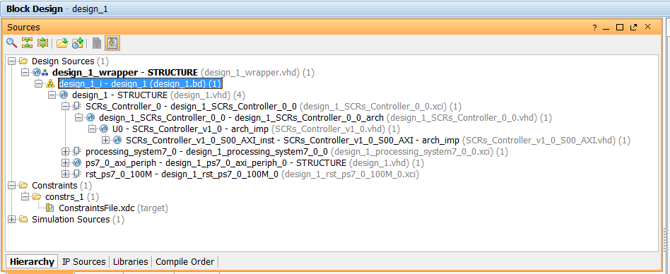 Figure2: Entire System VHDL files hierarchy
Before you generate bitstream file, you will need to add this constraints file: UCF.xdc Once you generate Bitstream file, export to the SDK and open an SDK project.
SDK Project
Once you generated the Bitstream file after following all the necessary steps as we did in the past tutorials. You can launch your SDK project and copy and paste the following source code in the Hello.c file. Also you can rename this file as well. I renamed this file: SRCs_Controller.c
#include "xparameters.h"
#include "xstatus.h"
#include "xil_printf.h"
#include "xuartps_hw.h"
#include "xbasic_types.h"
#include "math.h"
#include "platform.h"

#define BUFFER_SIZE 2
#define CyclesPerPeriod 2000000
#define ClockCycles 100000000

int ReceiveBuffer[BUFFER_SIZE]; /* Buffer for Transmitting Data */

Xuint32 *baseaddr_p = (Xuint32 *)XPAR_SCRS_CONTROLLER_0_S00_AXI_BASEADDR;

int sleep(unsigned int seconds);

int Calculate_RisingEdgeCounter(int *temp);

int main(void)
{

u8 counter=0;
int temp=0;

int RisingEdgeCounter=0;
int FallingEdgeCounter=0;
float tempvalue=0;

xil_printf("Enter a value between 0 and 90 degrees for phase delay: \n");

while(1)
{

if(XUartPs_IsReceiveData(STDIN_BASEADDRESS))
{
counter++;

if(counter==1)
{
ReceiveBuffer[0]=0;
ReceiveBuffer[1]=0;

ReceiveBuffer[0]=XUartPs_RecvByte(STDIN_BASEADDRESS); //receive data from terra term
}
else
{

ReceiveBuffer[1]=XUartPs_RecvByte(STDIN_BASEADDRESS); //receive data from terra term

temp=(ReceiveBuffer[0]-48)*10;
temp=temp+(ReceiveBuffer[1]-48);

xil_printf("phase angle delay value entered is: %d \n",temp);

//compute rising edge counter
RisingEdgeCounter= Calculate_RisingEdgeCounter(&temp);
xil_printf("RisingEdgeCounter is %d: \n",RisingEdgeCounter);

// compute falling edge counter
tempvalue=0.02/3;
FallingEdgeCounter=tempvalue*100000000;
xil_printf("FallingEdgeCounter is %d: \n",FallingEdgeCounter);

counter=0;
temp=0;

*(baseaddr_p+0) = RisingEdgeCounter;
xil_printf("register 0 is %d: \n",*(baseaddr_p+0));

*(baseaddr_p+1) = FallingEdgeCounter;
xil_printf("register 1 is %d: \n",*(baseaddr_p+1));

xil_printf("Enter a value between 0 and 90 degrees for phase delay: \n\n");
}


}
}

return 0;
}

int Calculate_RisingEdgeCounter(int *temp)
{
float tempvalue=0;

tempvalue=(*temp)*CyclesPerPeriod;
tempvalue=tempvalue/360;

return((int)tempvalue);
}
After you program your FPGA, and you run you C code, you can connect you oscilloscope probes to the Thyrstors GPIOs as defined on the UCF file and look at the six pluses generated after you define your phase delay from the serial port. Below are my results:
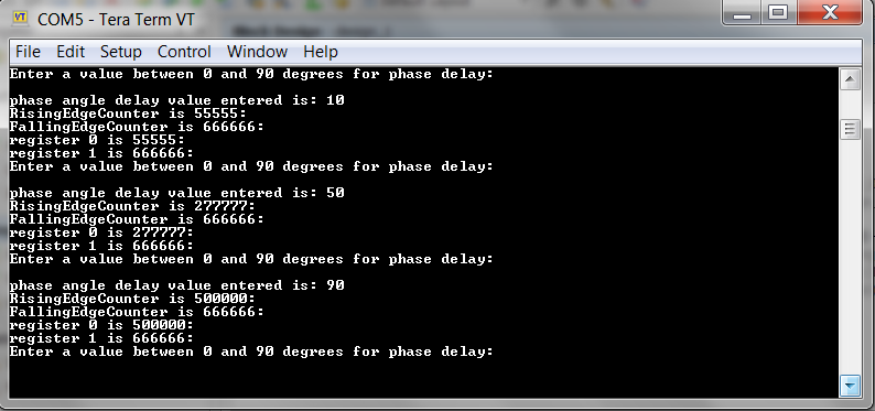 Figure3: Tera Term terminal showing rising edge and falling edge requests sent
Below are the corresponding screen shots taken per delay angle requested: 10, 50, and 90 degrees delays. You can notice that as the delay angle increases, the pulse width decreases and thus the DC output voltage. This true due to the fact the falling edge of the pulse always has to occur at 120 degrees from the zero crossing detect event. More info on this can be found my previous tutorial: Three Phase Full-Wave Controller Bridge Rectifier.
Also notice that all six pulses signals generated are 60 degrees out of phase of each other regardless of the phase delay requested.
Each individual pulse has a period of 360 degrees: meanin time difference between each rising edge per pluse is 320 degrees or 20 ms in the case of a 50Hz system.
Note: If the AC reference potential is the same as the neutral point potential of the three-phase voltage system, we have to add a 30 degrees phase shift to the delay angle: meaning if we have a delay of 10 degrees we have to fire the thyristor gate pulse at 40 degrees from the zero crossing detection event, unlike in our case where the pulse is sent exactky at 10 degrees from the zero crossing. Our test assumes that the AC system potential is not the same as the neutral potential.
 Figure3: 10 Degrees Phase Delay
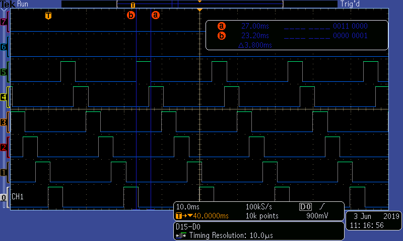 Figure4: 50 Degrees Phase Delay
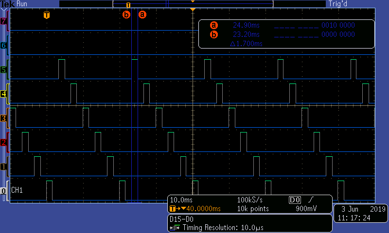 Figure5: 90 Degrees Phase Delay
Conclusion
This was just another example of how AXI4 can be used in your FPGA designs. I hope you have enjoyed this tutorial and learned more about how SCRs gate pulses are timed with respect to the zero crossing event.
Author: Farid M, https://embeddeddesign.org/
If you find any of the projects posted here helpful to you while working on similar projects, or you learned something from any of the topics discussed, please do not hesitate to make a donation, whatever amount you can afford, just as a gesture of appreciation and to keep this website alive and progressing so that its benefits extends to many younger engineers and students around the globe.
