
Introduction
In this project, I will demonstrate how amplitude modulation (AM) works using a practical digital implementation. The AM signal is generated using a Direct Digital Synthesis (DDS) approach implemented in Vivado. By controlling the amplitude of the carrier with a low-frequency message signal, this example illustrates the fundamental principles of AM modulation in a way that is easy to visualize and verify in simulation and hardware.
Disclaimer: AM transmission is illegal or strictly regulated in most countries. This project is intended for educational and simulation purposes only. Implementing this design on real hardware for over-the-air transmission is not encouraged and may violate local laws and regulations. Unchanged: local laws and regulations.
AM Modulation Theory
Amplitude Modulation (AM) Implementation
Amplitude modulation is implemented by varying the amplitude of a high-frequency carrier signal in proportion to a lower-frequency message (baseband) signal. In its simplest analog or digital form, this is achieved by multiplying the carrier waveform by the message signal after applying a suitable DC offset to ensure that the envelope remains positive. Mathematically, the AM signal can be written as:
s(t) = Ac[1 + m(t)] cos(2πfct)
Ac: is the carrier amplitude
m(t): is the normalized message signal
fc: is the carrier frequency
In digital implementations such as FPGA- or DSP-based systems, AM is commonly realized using a multiplier block to scale the carrier by the message signal, followed by an adder to include the carrier component. This method produces the characteristic AM spectrum consisting of the carrier and two sidebands located
at fc ± fm.
Modulation Sensitivity in Amplitude Modulation (AM)
In amplitude modulation (AM), the modulation sensitivity describes how strongly the amplitude of the carrier signal responds to changes in the amplitude of the modulating (message) signal. It defines the proportional relationship between the message signal and the resulting variation in the
carrier envelope.
The AM signal can be expressed mathematically as:
s(t) = Ac [ 1 + ka m(t) ] cos(2πfct)
where Ac is the carrier amplitude, m(t) is the message signal, fc is the carrier frequency, and ka is the amplitude modulation sensitivity.
Physically, the modulation sensitivity ka determines how much the carrier amplitude changes for a given change in the message signal amplitude. A larger value of ka results in deeper modulation, while a smaller value produces shallower modulation.
The AM modulation index, denoted by μ, is directly related to the modulation sensitivity and is given by:
μ = ka Am
where Am is the peak amplitude of the message signal. For μ < 1, the signal is under-modulated; for μ = 1, the signal is fully modulated; and for μ > 1, over-modulation occurs, causing envelope distortion.
In digital and FPGA-based AM implementations, the modulation sensitivity is realized as a scaling coefficient in a multiplier block that controls how the message samples modulate the carrier amplitude.
Implementation
In this implementation, a 1 kHz message tone is used to amplitude-modulate a 2 MHz carrier frequency. The goal is to demonstrate AM behavior. The message signal and carrier are both generated using DDS cores, ensuring precise frequency control. The digital operation implemented in this design follows the expression:
Modulated Signal s(t) = cos(2πfmt) × cos(2πfct) + cos(2πfct) ,
where the message tone is multiplied with the carrier and the carrier component is added back to form a conventional AM signal with a carrier present. This approach directly maps to a hardware implementation using a multiplier and adder, making it well suited for FPGA-based AM modulation experiments.
In this implementation the Amplitude modulation sensitivity and modulation index are assumed to be equal to 1: μ = 1.
VHDL code
The code below uses 200MHz frequency for the DDS clock. Also note the four clock delay used in the process at the end of the code. This is used to synchronize the inputs to the adder IP core. It takes 4 clock cycles for the multiplier to complete one multiplication computation. Also notice that product was scaled down to 16 signed bits and then added to the coresponding 16 bits of the carrier frequency sample.
  library IEEE;
use IEEE.STD_LOGIC_1164.ALL;
use IEEE.numeric_std.all;


entity AM_Modulator_TopLevel is
  port (
    sys_clk : in std_logic;
    reset   : in STD_LOGIC
  );
end AM_Modulator_TopLevel;

architecture behavioral of AM_Modulator_TopLevel is

signal clk200MHz                : std_logic;
signal clk400MHz                : std_logic;
signal locked_Sig               : std_logic;
signal DDS0_tvalid_out          : std_logic;
signal CarrierFrequency         : std_logic_vector(15 downto 0);
signal CarrierFrequency_dly     : std_logic_vector(15 downto 0);

signal DDS1_tvalid_out          : std_logic;
signal MultAdd_In_valid         : std_logic;
signal MessageTone_Signal       : std_logic_vector(15 downto 0);
signal MessageCarrierMultiplied : std_logic_vector(31 downto 0);
--signal PCOUT_Signal             : std_logic_vector(47 downto 0);
signal MessageCarrierMultipliedScaled  : std_logic_vector(15 downto 0);
signal AM_ModulatedSignal       : std_logic_vector(16 downto 0);


signal CarrierFrequency_dly1 : std_logic_vector(15 downto 0);
signal CarrierFrequency_dly2 : std_logic_vector(15 downto 0);
signal CarrierFrequency_dly3 : std_logic_vector(15 downto 0);
signal CarrierFrequency_dly4 : std_logic_vector(15 downto 0);

component clk_wiz_0
port
 (
  clk_out1          : out    std_logic;
  clk_out2          : out    std_logic;
  locked            : out    std_logic;
  clk_in1           : in     std_logic
 );
end component;


COMPONENT dds_compiler_0
  PORT (
    aclk : IN STD_LOGIC;
    m_axis_data_tvalid : OUT STD_LOGIC;
    m_axis_data_tdata : OUT STD_LOGIC_VECTOR(15 DOWNTO 0)
  );
END COMPONENT;

COMPONENT mult_gen_0
  PORT (
    CLK : IN STD_LOGIC;
    A : IN STD_LOGIC_VECTOR(15 DOWNTO 0);
    B : IN STD_LOGIC_VECTOR(15 DOWNTO 0);
    P : OUT STD_LOGIC_VECTOR(31 DOWNTO 0)
  );
END COMPONENT;

COMPONENT dds_compiler_1
  PORT (
    aclk : IN STD_LOGIC;
    m_axis_data_tvalid : OUT STD_LOGIC;
    m_axis_data_tdata : OUT STD_LOGIC_VECTOR(15 DOWNTO 0)
  );
END COMPONENT;

COMPONENT c_addsub_0
  PORT (
    A : IN STD_LOGIC_VECTOR(15 DOWNTO 0);
    B : IN STD_LOGIC_VECTOR(15 DOWNTO 0);
    CLK : IN STD_LOGIC;
    S : OUT STD_LOGIC_VECTOR(16 DOWNTO 0)
  );
END COMPONENT;


begin

Clk_Wizard: clk_wiz_0
   port map (
   clk_out1 => clk200MHz,
   clk_out2 => clk400MHz,
   locked => locked_Sig,
   clk_in1 => sys_clk
 );


DDS_0 : dds_compiler_0
  PORT MAP (
    aclk => clk200MHz,
    m_axis_data_tvalid => DDS0_tvalid_out,
    m_axis_data_tdata => CarrierFrequency
  );

 DDS1 : dds_compiler_1
 PORT MAP (
    aclk => clk200MHz,
    m_axis_data_tvalid => DDS1_tvalid_out,
    m_axis_data_tdata => MessageTone_Signal
  );

Multiplier : mult_gen_0
  PORT MAP (
    CLK => clk200MHz,
    A => CarrierFrequency,
    B => MessageTone_Signal,
    P => MessageCarrierMultiplied
  );


MessageCarrierMultipliedScaled  CarrierFrequency_dly4,
    B => MessageCarrierMultipliedScaled,
    CLK => clk200MHz,
    S => AM_ModulatedSignal
  );
 ----------------------------------------------------------------------
 -- This process is used to synchronize Muliplication and addition
 -- operation: it takes 4 clock cycles to complete one multiplication
 -----------------------------------------------------------------------
DELAY_PROC: process(clk200MHz)
begin
  if rising_edge(clk200MHz) then
    if reset = '1' then
      CarrierFrequency_dly1  '0');
      CarrierFrequency_dly2  '0');
      CarrierFrequency_dly3  '0');
      CarrierFrequency_dly4  '0');
    else
      CarrierFrequency_dly1 <= CarrierFrequency;
      CarrierFrequency_dly2 <= CarrierFrequency_dly1;
      CarrierFrequency_dly3 <= CarrierFrequency_dly2;
      CarrierFrequency_dly4 <= CarrierFrequency_dly3;
    end if;
  end if;
end process;
end behavioral;
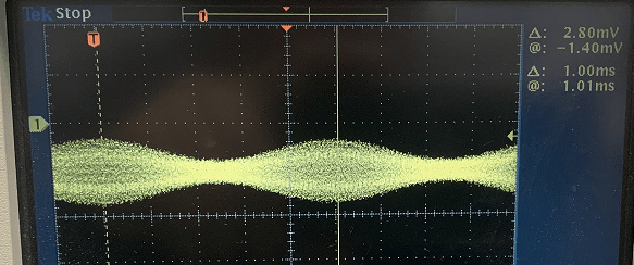
Vivado Simulation
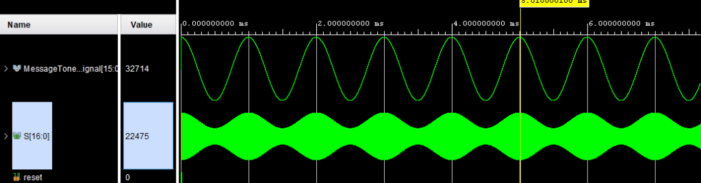
The simulation image below shows the modulated message signal. You can see the message signal envelop matches the message signal.
Source Code
For a complete copy of the source code, please send me a message or send me a request in the comments section below. I hope you will find this tutorial helpful, and I would really appreciate any feedback or comments.
Author: Farid M
