
Introduction
In this project, I demonstrate how to design an FIR filter using the Vivado FIR IP Core and validate the design using a frequency sweep generated by the Xilinx DDS IP Core. The DDS performs a sweep from DC to 100 kHz. More information about how DDS works and implemented in Vivado can be found in my previous posts.
The low pass filter to be design is a 12.5KHz filter and it is widely used for Narrow Band FM radios.
Theory
A Finite Impulse Response (FIR) filter is a class of digital filters whose output depends only on a finite number of present and past input samples. Unlike IIR filters, FIR filters do not use feedback, which guarantees stability and allows for exact linear-phase response when the coefficients are symmetric.
The output of an FIR filter is computed as a weighted sum of delayed input samples. Mathematically, the FIR filter output y[n] is given by:
y[n] = ∑k=0N-1 h[k] · x[n – k]
where x[n] is the input signal, h[k] are the FIR filter coefficients, and N is the number of taps (filter order + 1). Each coefficient represents the impulse response of the filter, and the convolution operation determines how different frequency components are attenuated or passed.
In the frequency domain, the FIR filter implements a frequency response H(ejω) that is defined by the discrete-time Fourier transform (DTFT) of the impulse response:
H(ejω) = ∑k=0N-1 h[k] e-jωk
By properly designing the coefficients h[k], the FIR filter can be made to operate as a low-pass, high-pass, band-pass, or band-stop filter. In this project, a low-pass FIR filter is designed to pass frequencies below 12.5 kHz while attenuating higher-frequency components with a stopband rejection of approximately 60 dB.
The sampling frequency fs determines the frequency resolution and transition bandwidth of the filter. With a sampling frequency of 1.5625 MHz, the normalized cutoff frequency is defined as:
fc,normalized = fc / fs
The FIR filter coefficients used in this design were generated using MATLAB’s Filter
Designer tool and imported into the Xilinx FIR Compiler IP core. The IP core performs
the multiply-accumulate (MAC) operations efficiently in hardware, producing one
filtered output sample for each asserted input tvalid signal.
FIR Filter Requirements
The FIR filter must meet the following specifications:
- Sampling frequency: 1.5625 MHz
- Cutoff frequency: 12.5 kHz
- Stopband frequency: 50 kHz
- Stopband ripple / attenuation: 60 dB
Implementation
To obtain the FIR filter coefficients, the MATLAB Filter Designer tool was used. The following settings were applied to generate the coefficients.
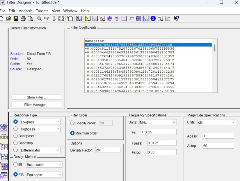
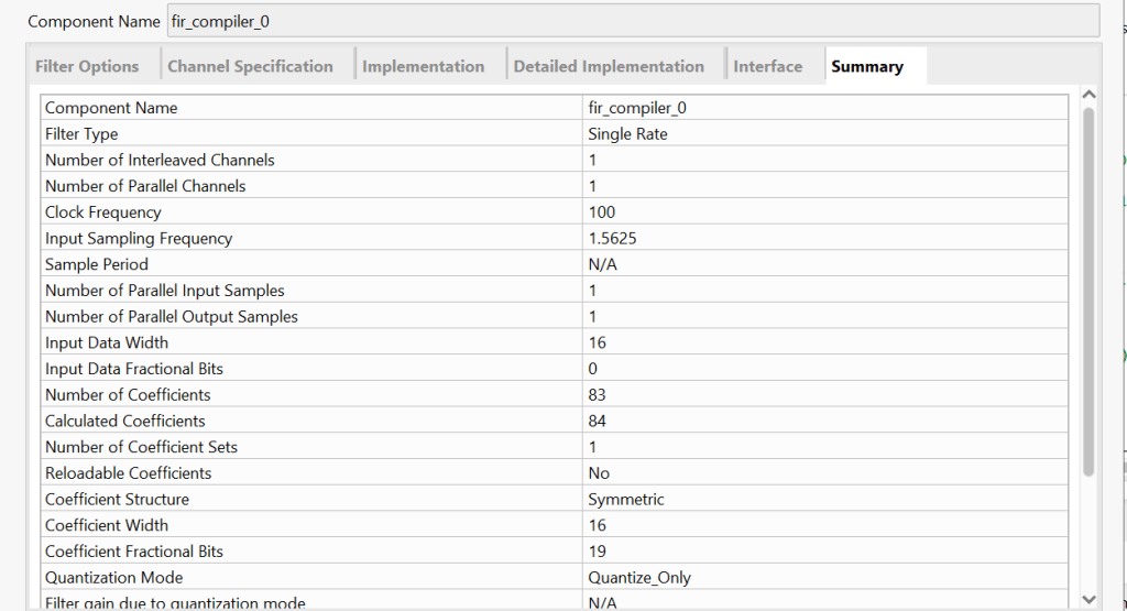
The tool generated 82 FIR coefficients, which were then imported into the Vivado FIR IP Core to implement the digital low-pass filter.
FIR Coefficients
Below are the FIR filter coefficients generated by the MATLAB Filter Designer and used in the Vivado FIR IP Core:
| Column 1 | Column 2 | Column 3 | Column 4 |
|---|---|---|---|
| -0.000967862 | -0.0000481134 | -0.00000466235 | 0.0000726547 |
| 0.000188582 | 0.000346709 | 0.000552722 | 0.000811463 |
| 0.001127683 | 0.001506278 | 0.001951862 | 0.002468238 |
| 0.003058989 | 0.003726425 | 0.004472287 | 0.005297174 |
| 0.00620074 | 0.007181225 | 0.00823595 | 0.009360603 |
| 0.010549998 | 0.011797438 | 0.013095198 | 0.014434148 |
| 0.015804338 | 0.017194453 | 0.018592739 | 0.019986384 |
| 0.021362336 | 0.022707065 | 0.024007213 | 0.02524909 |
| 0.026419772 | 0.027506082 | 0.028495994 | 0.029378269 |
| 0.030143046 | 0.030781337 | 0.031286852 | 0.031651157 |
| 0.031871198 | 0.031945967 | 0.031871198 | 0.031651157 |
| 0.031286852 | 0.030781337 | 0.030143046 | 0.029378269 |
| 0.028495994 | 0.027506082 | 0.026419772 | 0.02524909 |
| 0.024007213 | 0.022707065 | 0.021362336 | 0.019986384 |
| 0.018592739 | 0.017194453 | 0.015804338 | 0.014434148 |
| 0.013095198 | 0.011797438 | 0.010549998 | 0.009360603 |
| 0.00823595 | 0.007181225 | 0.00620074 | 0.005297174 |
| 0.004472287 | 0.003726425 | 0.003058989 | 0.002468238 |
| 0.001951862 | 0.001506278 | 0.001127683 | 0.000811463 |
| 0.000552722 | 0.000346709 | 0.000188582 | 0.0000726547 |
| -0.00000466235 | -0.0000481134 | -0.000967862 |
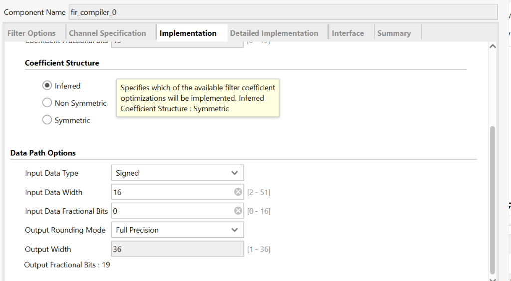
Vivado FIR Compiler Setup
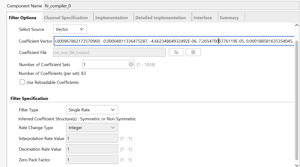
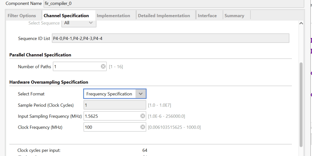
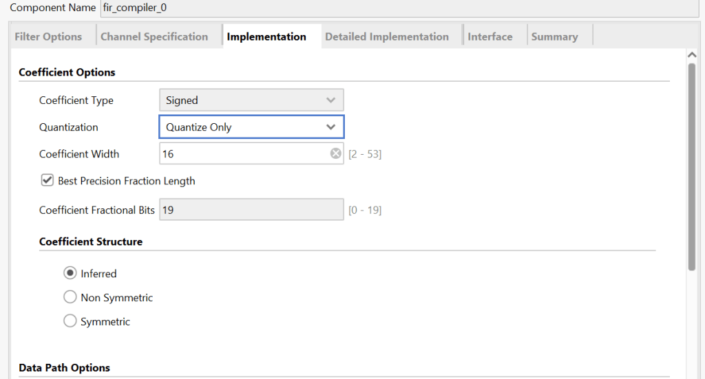
Vivado 2020.2 was used to configure and generate the FIR filter using the Xilinx FIR Compiler IP Core. From the IP Catalog, the FIR Compiler IP was selected and configured according to the previously defined filter requirements. The following screenshots illustrate the configuration process.
The screenshot below shows how the FIR coefficients are entered into the Coefficient Vector field. The coefficients are comma-separated, and a total of 83 coefficients were used.


VHDL Implementation
Below is the top-level VHDL design used to implement the system. The design instantiates the following main digital blocks:
- Clock Wizard
- FIR Compiler IP Core
- DDS IP Core
The Clock Wizard generates a 100 MHz system clock from the on-board 125 MHz oscillator. This 100 MHz clock is used by both the FIR Compiler and DDS IP cores. The effective sampling frequency used by the FIR filter is 1.5625 MHz.
library ieee;
use ieee.std_logic_1164.all;
use IEEE.STD_LOGIC_UNSIGNED.ALL;
use ieee.numeric_std.all;

Library UNISIM;
use UNISIM.vcomponents.all;

entity FIR_TopLevel is
port (
   clk_p       : in  STD_LOGIC;
   clk_n       : in  STD_LOGIC;

   reset       : in  std_logic;                -- Reset signal

   FIR_Out     : out std_logic_vector(15 downto 0)
);
end FIR_TopLevel;

architecture Behavioral of FIR_TopLevel is

signal clk                : std_logic := '0';
signal clk_aux            : std_logic := '0';

signal Clk_6p25MHz        : std_logic := '0';
signal Clk_100MHz         : std_logic := '0';
signal lockedSig          : std_logic := '0';

signal DDS_data_tvalid_out : std_logic := '0';
signal DDS_data_tdata_out  : std_logic_vector(15 DOWNTO 0);

signal clockcounter : integer range 0 to 4;
signal FIR_sample_valid_in     : std_logic := '0';       -- Sample valid input signal
signal s_axis_data_tready_Sig  : STD_LOGIC;
signal m_axis_data_tvalid_Sig  : STD_LOGIC;
signal m_axis_data_tdata_Sig   : STD_LOGIC_VECTOR(39 DOWNTO 0);

component clk_wiz_0
port
 (
  clk_out1          : out    std_logic;
  clk_out2          : out    std_logic;

  locked            : out    std_logic;
  clk_in1           : in     std_logic
 );
end component;

component DDS_Sweep
port (
   clk             : in std_logic := '0';  --system cock running at 399.68MHz
   reset           : in std_logic;

   DDS_data_tvalid : OUT STD_LOGIC;
   DDS_data_tdata  : OUT STD_LOGIC_VECTOR(15 DOWNTO 0)
);
end component;

COMPONENT fir_compiler_0
  PORT (
    aclk : IN STD_LOGIC;
    s_axis_data_tvalid : IN STD_LOGIC;
    s_axis_data_tready : OUT STD_LOGIC;
    s_axis_data_tdata : IN STD_LOGIC_VECTOR(15 DOWNTO 0);
    m_axis_data_tvalid : OUT STD_LOGIC;
    m_axis_data_tdata : OUT STD_LOGIC_VECTOR(39 DOWNTO 0)
  );
END COMPONENT;

begin


-- Instantiate the differential clock buffer
ibufds_inst : IBUFDS
   port map (
    I  => clk_p,
    IB => clk_n,
    O  => clk_aux --125MHz
);


-- Global Clock Buffer
clk_buf : BUFG port map (
    I => clk_aux,
    O => clk
);

ClockWiZ: clk_wiz_0
   port map (
   clk_out1 => Clk_6p25MHz,
   clk_out2 => Clk_100MHz,

   locked => lockedSig,

   clk_in1 => clk
 );

DDS_Inst: DDS_Sweep
port map(
   clk             => Clk_100MHz,
   reset           => reset,

   DDS_data_tvalid => DDS_data_tvalid_out,
   DDS_data_tdata  => DDS_data_tdata_out
);

FIR_IPcore: fir_compiler_0
  PORT MAP (
    aclk => Clk_100MHz,
    s_axis_data_tvalid => FIR_sample_valid_in,
    s_axis_data_tready => s_axis_data_tready_Sig,
    s_axis_data_tdata => DDS_data_tdata_out,
    m_axis_data_tvalid => m_axis_data_tvalid_Sig,
    m_axis_data_tdata => m_axis_data_tdata_Sig
  );

FIR_Out <= m_axis_data_tdata_Sig(39 downto 24);

--this process is used to generate the valid input data for the FIR.
process(Clk_6p25MHz,reset)
variable index: integer:= 0;
begin
     if(reset='1') then
         clockcounter<=0;
         FIR_sample_valid_in<='0';
     elsif(rising_edge(Clk_6p25MHz)) then
         clockcounter <=clockcounter+1;
             if (clockcounter=3) then
                 FIR_sample_valid_in <='1';
                 clockcounter<=0;
             else
                 FIR_sample_valid_in <='0';
             end if;
     end if;
end process;


end Behavioral;
The process at the end of the code is used to generate the
tvalid signal for the FIR input. This signal defines the effective
sampling frequency (fs) of the filter and is set to
1.5625 MHz.
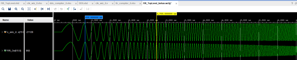
Vivado Simulation and Filter Validation With DDS
Vivado simulation tool was used to validate the frequency response of the filter. With the help of Xilinix DDS that performed a frequency sweep from DC to 100KHz, we could see in the image taken below that input frequency coming in from DDS into the FIR filter starts to attenuate roughly around 13KHz.
In the next project, I plan to demonstrate the performance of this filter in the real world using and signal generator and an FPGA development board.
For access to the source code, you can clone a copy from my Github repository in the link below.
Source code:
https://github.com/faridfma/FIR_12K5_DDS
I hope you will find this tutorial helpful, and I would really appreciate any feedback or comments in the comments section and via emails.
